Wafer bonding method and preparation method for foreign substrate

A technology of wafer bonding and heterogeneous substrates, applied in welding equipment, manufacturing tools, optomechanical equipment, etc., can solve problems such as thermal expansion coefficient mismatch, heterogeneous bonding structure fragmentation, bonding structure debonding, etc. Achieve the effects of improving reliability, reducing thermal strain, and expanding the scope of use

Active Publication Date: 2017-05-24
SHANGHAI NOVEL SI INTEGRATION TECH CO LTD
View PDF11 Cites 25 Cited by
  • Summary
  • Abstract
  • Description
  • Claims
  • Application Information

AI Technical Summary

Problems solved by technology

However, due to the thermal expansion coefficient mismatch between heterogeneous materials, heterogeneous bonding structures will generate huge thermal strains under high-temperature processes such as high-temperature reinforcement, defect recovery, and material film transfer.
Thermal strain may lead to debonding of the bonded structure or even fragmentation of the heterogeneous bonded structure, making it impossible to achieve a wide range of heterogeneous integration

Method used


Image

  • Wafer bonding method and preparation method for foreign substrate
  • Wafer bonding method and preparation method for foreign substrate
  • Wafer bonding method and preparation method for foreign substrate

Examples


Embodiment 1

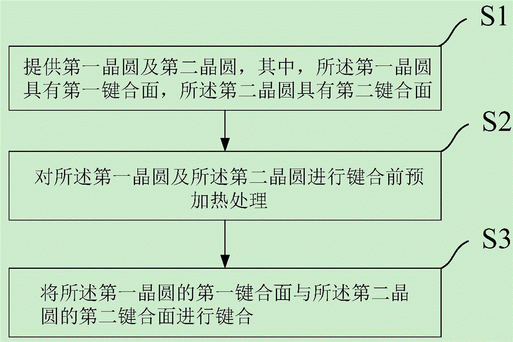
[0039] see figure 1 , the present invention provides a wafer bonding method, the method at least comprising:

[0040] S1: providing a first wafer and a second wafer, wherein the first wafer has a first bonding surface, and the second wafer has a second bonding surface;

[0041] S2: Pre-heating the first wafer and the second wafer before bonding;

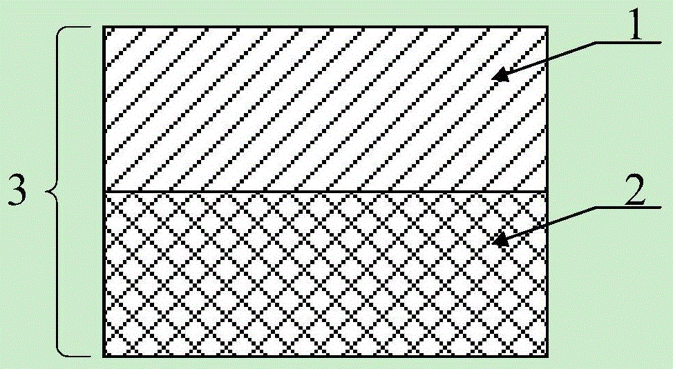
[0042] S3: Bonding the first bonding surface of the first wafer to the second bonding surface of the second wafer;

[0043] The wafer bonding method of the present invention will be described in detail below with reference to specific drawings.

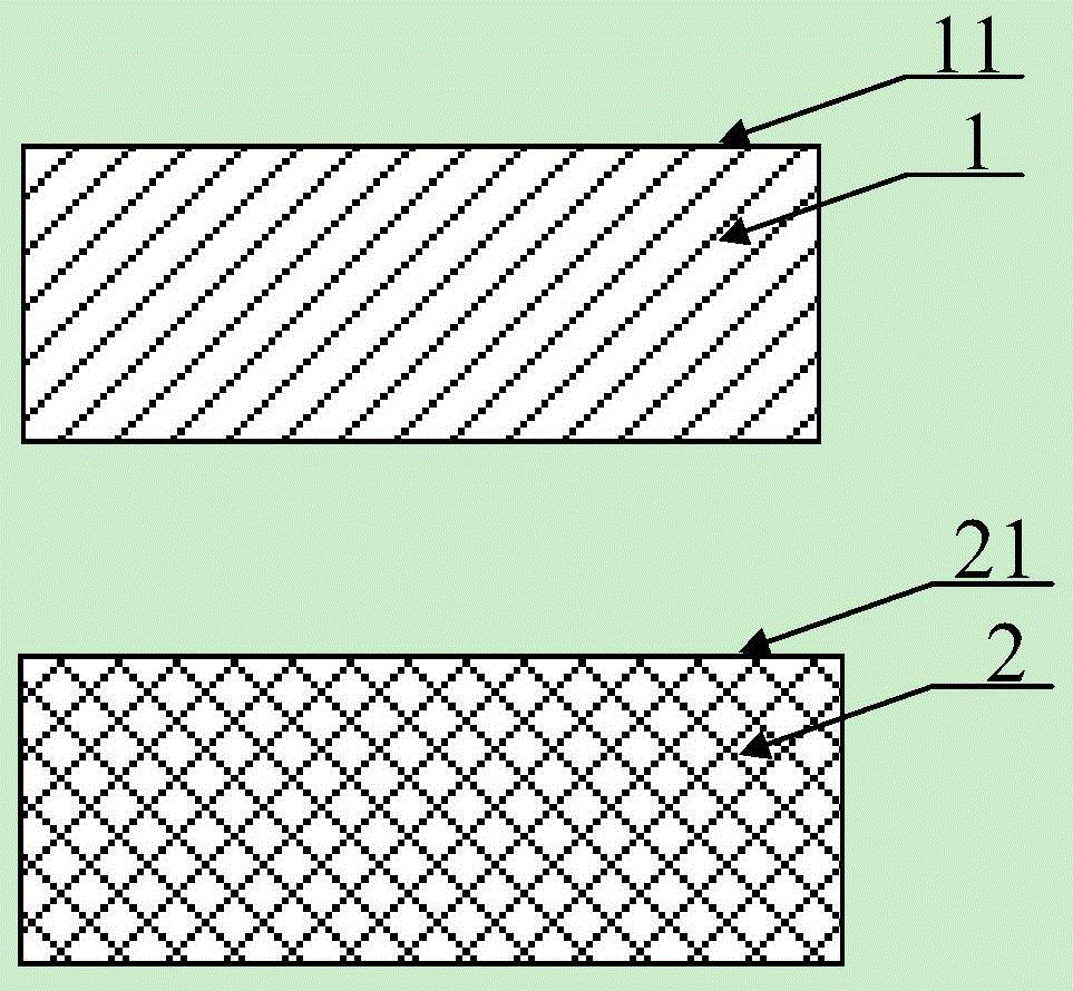
[0044] see figure 1 S1 and figure 2 , performing step S1, providing a first wafer 1 and a second wafer 2, wherein the first wafer 1 has a first bonding surface 11, and the second wafer 2 has a second bonding surface 21;

[0045] Specifically, the first wafer 1 has an upper surface and a lower surface, which can be used as the first bonding surface 11; the second wafer 2 has an upper su...

Embodiment 2

[0071] The present invention also provides a method for preparing a heterogeneous substrate, the preparation method at least includes: adopting the steps included in the wafer bonding method described in any one of the solutions in Embodiment 1, and also includes;

[0072] Before the heat treatment, ion implantation is performed on the first bonded surface 11 or the second bonded surface 21, so that at the preset depth of the first wafer 1 or the second wafer 2 Form a defective layer;

[0073] The first annealing treatment is performed on the structure having the defect layer obtained through the wafer bonding method, so as to peel part of the wafer along the defect layer.

[0074] Specifically, the first treatment is preferably carried out in a vacuum environment or under N 2 , O 2 , Ar, He, H 2 . Carry out under a protective atmosphere formed by at least one gas in the air, the temperature of the annealing treatment is 50°C-1300°C, and the time of the annealing treatment ...


PUM


Abstract

The invention provides a wafer bonding method and a preparation method for a foreign substrate. The wafer bonding method at least comprises the following steps: S1) supplying a first wafer and a second wafer, wherein the first wafer is equipped with a first bonding surface, and the second wafer is equipped with a second bonding surface; S2) preheating before bonding the first wafer and the second wafer; and S3) bonding the first bonding surface of the first wafer with the second bonding surface of the second wafer. According to the scheme, the preheating before the bonding for the wafers is capable of effectively reducing the thermal strain of the foreign bonding structure in a high-temperature post-annealing process, so that the use scope of the foreign bonding can be widened and the reliability of a foreign integrated material can be promoted. Meanwhile, the problems of de-bonding and broken bonding structure caused by thermal strain of the foreign bonding structure in the high-temperature post-annealing process can be solved.

Description

technical field [0001] The invention belongs to the field of material structure process preparation, and in particular relates to a wafer bonding method and a heterogeneous substrate preparation method. Background technique [0002] As the development of Moore's Law has encountered a bottleneck, a single material can no longer meet the rapid development of semiconductor technology. More than Moore's technology development route puts forward an urgent need for heterogeneous integration technology, which integrates materials with different properties to achieve high-density integration of multiple functional devices. For example, the integration of GaN and Si realizes the integration of GaN-based high electron mobility devices and silicon-based integrated circuits, and the integration of piezoelectric materials and Si realizes the integration of filter devices and integrated circuits. [0003] At present, the bonding process is widely used in the field of semiconductor materi...

Claims


Application Information

Patent Timeline
Patent Type & Authority Applications(China)
IPC IPC(8): H01L21/02H01L21/762B81C3/00
CPCB81C3/001H01L21/02104H01L21/76251
Inventor 黄凯欧欣张润春游天桂王曦
Owner SHANGHAI NOVEL SI INTEGRATION TECH CO LTD
Why Eureka
Try Eureka