Deep ultraviolet optics wave aberration detection apparatus and method

An optical system and detection device technology, applied in the field of optical measurement, can solve the problems of wave aberration detection difficulty, energy utilization rate, signal-to-noise ratio, and detection accuracy need to be improved, so as to improve the laser damage threshold and realize fast and high-precision detection , the effect of uniform spot

Active Publication Date: 2017-05-31
INST OF MICROELECTRONICS CHINESE ACAD OF SCI
View PDF9 Cites 11 Cited by
  • Summary
  • Abstract
  • Description
  • Claims
  • Application Information

AI Technical Summary

Problems solved by technology

[0004] U.S. Patents US6975387, US6914665 and the document "Portable phase measuring interferometer using Shack‐Hartmann method" (Proc. SPIE, 2003, 5038: 726~732) provide the method of measuring the wave of deep ultraviolet lithography objective lens by Shack‐Hartmann wavefront sensor. A device and a measurement method for aberration, but the device requires a collimating objective lens with a large numerical aperture, which brings difficulties to the detection of wave aberration
Chinese patent CN1016092668 effectively overcomes the difficulties caused by large numerical aperture collimating objective lenses by integrating the host and the first standard mirror on the mask stage and the second standard mirror on the silicon wafer stage, but the energy utilization rate of the system , signal-to-noise ratio, and detection accuracy all need to be improved

Method used


Image

  • Deep ultraviolet optics wave aberration detection apparatus and method
  • Deep ultraviolet optics wave aberration detection apparatus and method
  • Deep ultraviolet optics wave aberration detection apparatus and method

Examples


Embodiment Construction

[0033] Exemplary embodiments of the present disclosure will be described in more detail below with reference to the accompanying drawings. Although exemplary embodiments of the present disclosure are shown in the drawings, it should be understood that the present disclosure may be embodied in various forms and should not be limited by the embodiments set forth herein. Rather, these embodiments are provided for more thorough understanding of the present disclosure and to fully convey the scope of the present disclosure to those skilled in the art.

[0034] Embodiments of the present invention will be described in detail below in conjunction with the accompanying drawings.

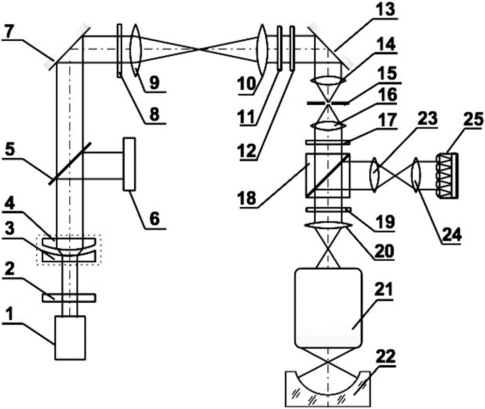
[0035] like figure 1 As shown, the wave aberration detection device of the deep ultraviolet optical system of the present invention includes an excimer laser (1), an energy controller (2), a plano-concave cylindrical mirror (3), a plano-convex cylindrical mirror (4), beam splitter (5), energy detector (6),...


PUM

PropertyMeasurementUnit
Laser damage thresholdaaaaaaaaaa

Abstract

The invention discloses a deep ultraviolet optics wave aberration detection apparatus and method; the apparatus comprises a quasi-molecular laser (1), an energy controller (2), a plano-concave cylindrical lens (3), a plano-convex cylindrical lens (4), a beam splitter (5), an energy detector (6), a first plane reflector (7), a diffractive optical element (8), a Fourier lens (9), a first collimating objective (10), a first 1 / 4 wave plate (11), a first 1 / 2 wave plate (12), a second plane reflector (13), a first focusing objective (14), an orifice plate (15), a second collimating objective (16), a second 1 / 2 wave plate (17), a polarizing splitting prism (18), a second 1 / 4 wave plate (19), a second focusing objective (20), a deep ultraviolet optical system (21) to be detected, a spherical reflector (22), a first relay lens (23), a second relay lens (24) and a Shack-Hartmann wavefront sensor (25). The deep ultraviolet optics wave aberration detection apparatus and method provide high-speed high-precision detection of system wave aberrations in integrated assembly and adjustment of deep ultraviolet optics.

Description

technical field [0001] The invention relates to the technical field of optical measurement, in particular to a device and method for detecting wave aberration of a deep ultraviolet optical system using the Shack-Hartmann method. Background technique [0002] In the field of scientific research and industry, optical systems working in the deep ultraviolet band play an increasingly important role, such as projection optical systems for semiconductor microlithography, observation systems used in the semiconductor industry, and micro-nano structure manufacturing processes The ultraviolet optical system used in the optical system, etc., these optical systems working in the deep ultraviolet band usually require extremely small wave aberration (on the order of several nanometers). Therefore, these optical systems must be tested for wave aberration in all aspects of processing, integration and work. [0003] The wave aberration detection methods of the deep ultraviolet optical syst...

Claims


Application Information

Patent Timeline
IPC IPC(8): G01M11/02G02B27/28G02B27/09
CPCG01M11/0242G02B27/0911G02B27/0927G02B27/0955G02B27/0966G02B27/283G02B27/286
Inventor 卢增雄齐月静苏佳妮齐威王宇周翊
Owner INST OF MICROELECTRONICS CHINESE ACAD OF SCI
Why Eureka
Try Eureka