An integrated photoelectric storage device based on phase-change nanowires and its testing method
An integrated optical and testing method technology, applied in the field of nano-devices, to achieve the effects of good reliability, low power, and low melting point
- Summary
- Abstract
- Description
- Claims
- Application Information
AI Technical Summary
Problems solved by technology
Method used
Image
Examples
Embodiment 1
[0023] in Si 3 N 4 / SiO 2 / Si substrates are prepared in two steps by electron beam-exposure etching process, that is, first on Si 3 N 4 / SiO 2 / Si to prepare the electrodes and alignment marks, the electrodes are Cr(10nm) / Au(90nm) structure, the total thickness is 100nm, and then the waveguide and vertical grating coupler are prepared by electron beam-exposure etching process again, and the electrodes are distributed in both sides of the waveguide. Finally, the GeTe nanowires were transferred onto Cr / Au electrodes, suspended vertically just above the waveguide. The waveguide width of the device is 1.3μm, the thickness is 200nm, the distance between the electrode and the waveguide is 300nm, and the short and long sides of the trapezoidal electrode are 4 and 20μm, respectively. The grating period of the vertical coupler is 1.14-1.16 μm, the fill factor is 0.88, and its coupling efficiency is about 27%. The length of the GeTe nanowire is about 26 μm, the diameter is 700 n...
Embodiment 2
[0025] Same as Example 1, the difference lies in that the waveguide suspended from the device has a width of 1.4 μm and a thickness of 300 nm, the distance between the electrode and the waveguide is 500 nm, and the short side of the trapezoidal electrode is 5 μm. The GeTe nanowires have a length of about 3 μm and a diameter of 300 nm. The laser write pulse wavelength is 1.56μm, the power consumption is 5.2mW, and the detection light wavelength is 1.57μm.
Embodiment 3
[0027] Same as embodiment 1, the difference lies in that the distance between the electrode and the waveguide is 1 μm, and the short side of the trapezoidal electrode is 5 μm. The GeTe nanowires have a length of about 12 μm and a diameter of 400 nm. Focused ion beam (FIB) was used to plate Pt at the contact between the nanowire and the electrode to improve the ohmic contact between the nanowire and the electrode. At this time, the resistance of the device in the crystalline state was 1.2KΩ.
[0028] 2. Analysis of Experimental Results
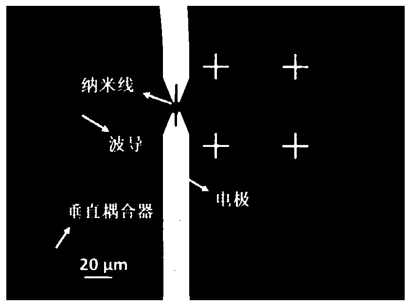
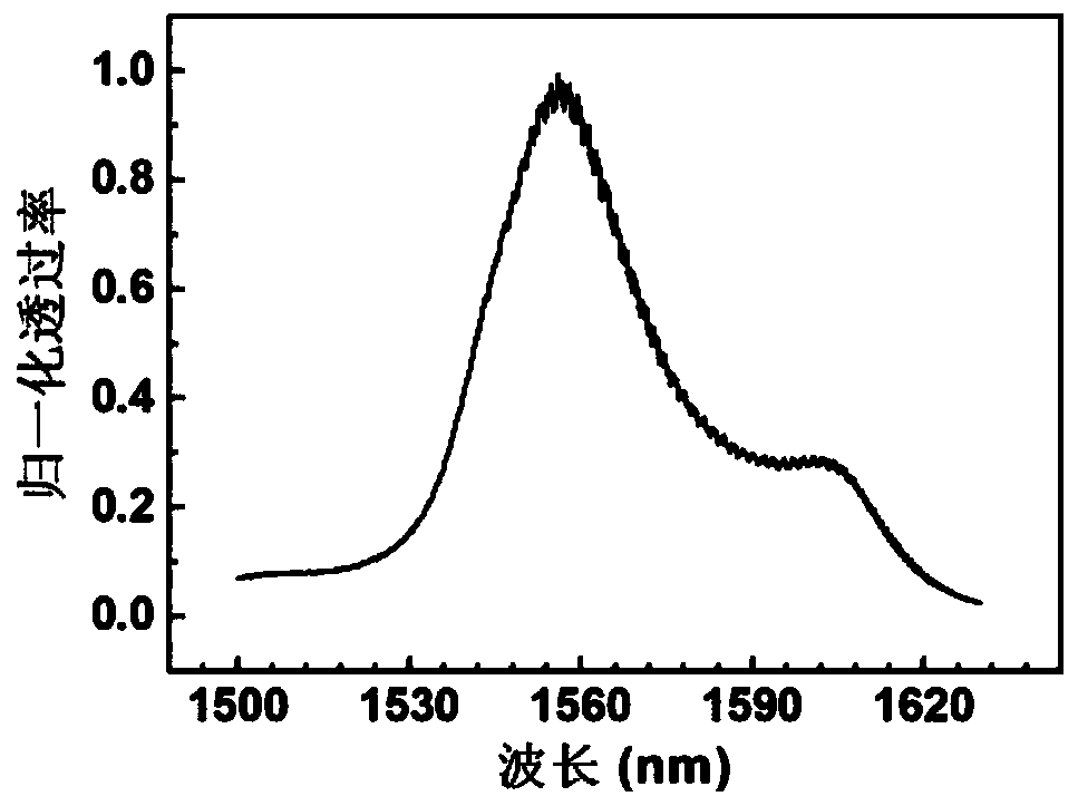
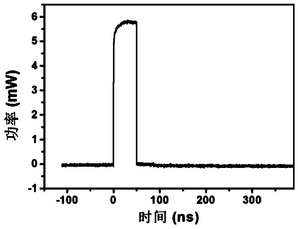
[0029] figure 1 It is an optical microscope picture of the device of the present invention. The device is mainly composed of Si 3 N 4 The waveguide, the Cr / Au electrodes on both sides of the waveguide, the vertical grating coupler connected to both ends of the waveguide and the GeTe nanowires connected to the two electrodes. The diameter of the GeTe nanowire is about 700nm, the length is about 26μm, and its direction is perpendicular to th...
PUM
 Abstract
Description
Claims
Application Information


