Substrate etching method

A substrate and a technology to be etched, applied in the field of microelectronics, can solve the problems of line width shrinkage at the bottom of deep holes, etching termination, and difficulty in discharging etching reactants, etc., to protect the side walls of deep holes and reduce line width The effect of loss and increase of etching depth

Inactive Publication Date: 2017-05-31
BEIJING NAURA MICROELECTRONICS EQUIP CO LTD
View PDF7 Cites 1 Cited by
  • Summary
  • Abstract
  • Description
  • Claims
  • Application Information

AI Technical Summary

Problems solved by technology

However, with the increase of etching depth, the entry of etching gas and the discharge of etching reactants in deep holes become relatively difficult. At this time, the C 4 f 8 The resulting polymer deposits on the sidewall and bottom of the pattern will instead cause the line width at the bottom of the deep hole to shrink, and even cause the etching to stop, so that the etching depth and morphology required by the process cannot be achieved.

Method used


Image

  • Substrate etching method
  • Substrate etching method
  • Substrate etching method

Examples


Embodiment Construction

[0035] In order to enable those skilled in the art to better understand the technical solution of the present invention, the substrate etching method provided by the present invention will be described in detail below in conjunction with the accompanying drawings.

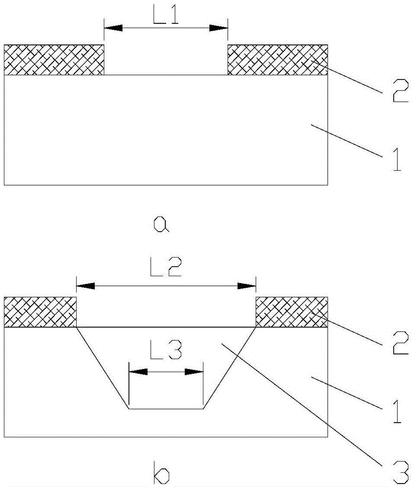
[0036] image 3 A flow chart of the substrate etching method provided by the present invention. see image 3 , the substrate etching method provided by the present invention is used to etch deep holes on the surface to be etched of a silicon dioxide substrate, comprising the following steps:

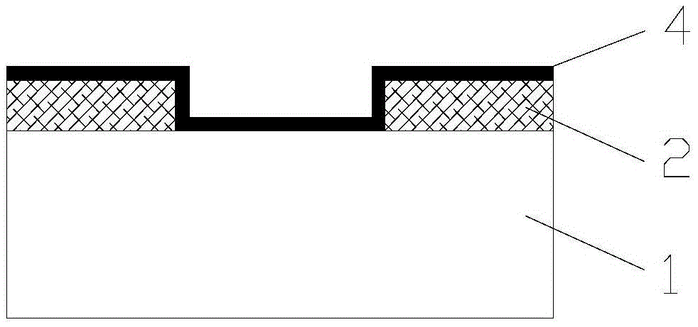
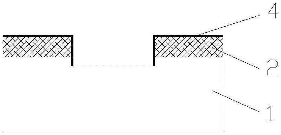
[0037] In the deposition step S1, a layer of polymer is deposited on the sidewall and bottom of the pattern by using fluorocarbon gas as the deposition gas.

[0038] In the etching step S2 , the anisotropic etching is performed by using the fluorine-containing gas whose etching product is the gas as the main etching gas and the inert gas as the auxiliary gas, so as to increase the etching depth of the deep hole.

[0039] T...


PUM


Abstract

The present invention provides a substrate etching method. The method is configured to etch a deep hole at the surface to be etched of a silicon dioxide substrate, and comprises the following steps: an etching step: employing the fluorine-containing gas which has an etching product being gas as the main etching gas and employing the inert gas as auxiliary gas to perform anisotropic etching so as to increase the etching depth; a deposition step: employing the fluorocarbon gas as the deposition gas to respectively deposit one layer of polymer at the side wall of the deep hole and the bottom of the deep hole; and circulation of the two steps mentioned above until reaching the required total etching depth. The substrate etching method allows the etching of the deep hole to be performed at the consistent temperature so as to avoid the prolonging of the whole etching time caused by the temperature difference, improve the average etching rate and fit the technology volume production.

Description

technical field [0001] The invention relates to the technical field of microelectronics, in particular to a substrate etching method. Background technique [0002] Compared with TSV technology, TGV (Through Glass Via, glass via) technology has the same advantages, and the glass substrate (silicon dioxide) has good micromachining performance, electrical, thermal mechanical properties and low cost, so that The advantages of TGV technology are more prominent, and it is known as the most promising three-dimensional packaging technology after TSV. To realize the TGV technology, the key point is that it is necessary to etch a high-aspect-ratio, small-sized through-hole structure on the glass substrate. [0003] The difficulty of etching deep holes on silicon dioxide substrates relative to shallow holes lies in: assuming that the pattern line width of mask 2 is L1, such as figure 1 As shown in figure a. A deep hole 3 is etched on the surface to be etched of the silicon dioxide s...

Claims


Application Information

Patent Timeline
IPC IPC(8): H01L21/311
Inventor 钦华林
Owner BEIJING NAURA MICROELECTRONICS EQUIP CO LTD
Why Eureka
Try Eureka