Semiconductor device and manufacturing method thereof

A device manufacturing method and semiconductor technology, which are applied in the fields of semiconductor/solid-state device manufacturing, semiconductor devices, electrical components, etc., can solve the problems of device line distortion, increasing device complexity, and local lattice defects.

Active Publication Date: 2020-07-07
INST OF MICROELECTRONICS CHINESE ACAD OF SCI
View PDF5 Cites 0 Cited by
  • Summary
  • Abstract
  • Description
  • Claims
  • Application Information

AI Technical Summary

Problems solved by technology

Compared with the aforementioned method, although this method reduces the distribution of SiGe and Ge materials on the entire wafer, that is, the growth of some local spaces to a certain extent, as long as the fin structure on the top of the STI is exposed, the Ge epitaxial layer will grow. For other device regions on the wafer that need to further improve the electron mobility, it is difficult to adopt a CMOS compatible process to manufacture in one step, that is, an additional mask photolithography / etching process is often required, which increases the complexity of the device and easily causes device lines. Distortion, and even device failure
In addition, since the bottom of the fin structure is monocrystalline silicon (bulk Si or SOI top monocrystalline silicon) during epitaxial growth, and the STI on both sides of the epitaxial layer is amorphous oxide, it is easy to produce localized silicon during the epitaxial process. Lattice defects

Method used


Image

  • Semiconductor device and manufacturing method thereof
  • Semiconductor device and manufacturing method thereof
  • Semiconductor device and manufacturing method thereof

Examples


Embodiment Construction

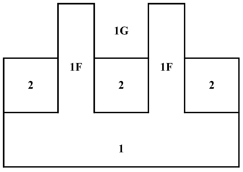
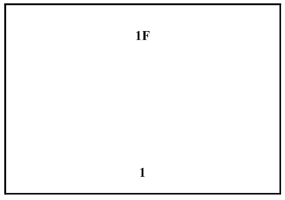
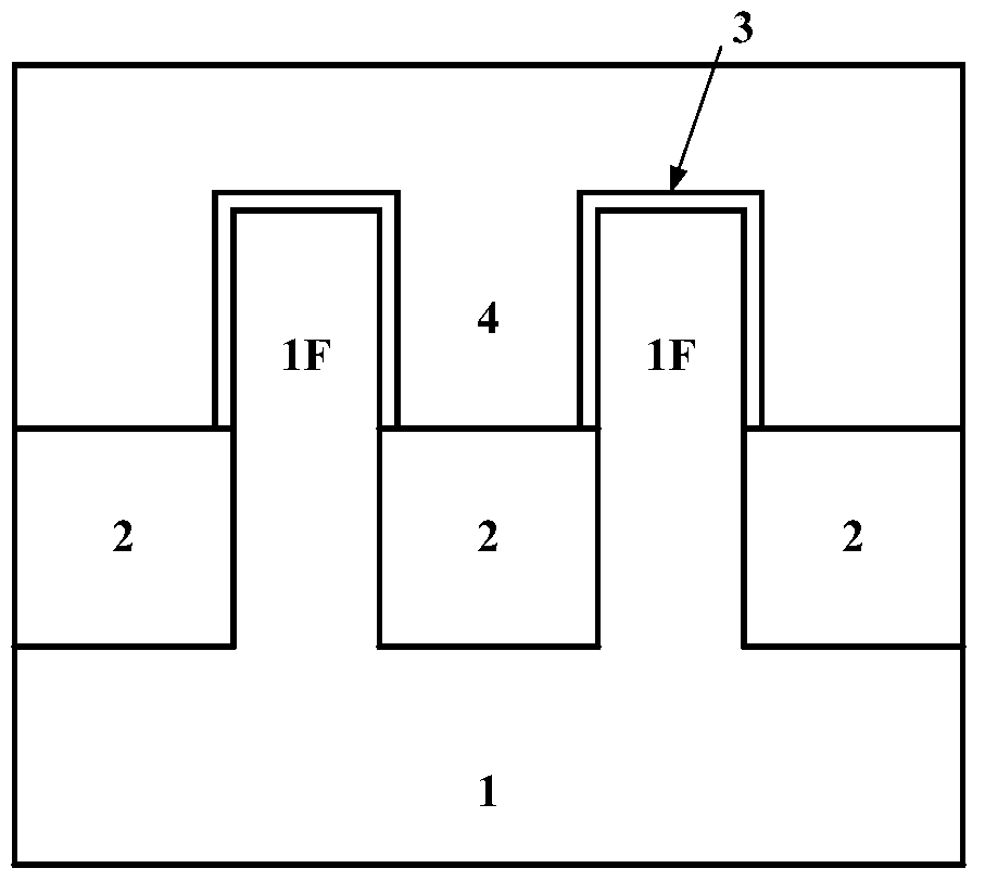
[0024] The characteristics and technical effects of the technical solution of the present invention will be described in detail below with reference to the accompanying drawings and in conjunction with schematic embodiments, which discloses a three-dimensional multiple Gate FinFET and method of manufacturing the same. It should be pointed out that similar reference numerals represent similar structures, and the terms "first", "second", "upper", "lower" and the like used in this application can be used to modify various device structures or manufacturing processes . These modifications do not imply spatial, sequential or hierarchical relationships of the modified device structures or fabrication processes unless specifically stated.

[0025] It is worth noting that the following figure A is a cross-sectional view along the direction perpendicular to the channel (along the second direction), and certain figure B is a cross-sectional view along the direction parallel to the chan...


PUM


Abstract

The invention discloses a semiconductor device, comprising: a plurality of fins extending along a first direction on a substrate, extending along a second direction and crossing the gate of each fin, The source-drain region and the side wall of the gate, wherein the fin is composed of a buffer layer and a channel layer made of high-mobility material, and the buffer layer surrounds the side surface and the bottom surface of the channel layer. According to the semiconductor device and its manufacturing method of the present invention, by removing the dummy gate stack while increasing the etching depth and lateral width, a high carrier mobility can be locally aligned on the desired fin structure channel, thereby effectively improving the carrier mobility in the channel region of the fin, thereby effectively improving device performance and reliability.

Description

technical field [0001] The invention relates to a semiconductor device and a manufacturing method thereof, in particular to a three-dimensional multi-gate FinFET with high carrier mobility and a manufacturing method thereof. Background technique [0002] In the current sub-20nm technology, the three-dimensional multi-gate device (FinFET or Tri-gate) is the main device structure, which enhances the gate control capability and suppresses leakage and short channel effects. [0003] For example, compared with traditional single-gate bulk Si or SOI MOSFETs, MOSFETs with double-gate SOI structures can suppress short-channel effects (SCE) and drain-induced barrier lowering (DIBL) effects, have lower junction capacitance, and can To achieve light channel doping, the threshold voltage can be adjusted by setting the work function of the metal gate, which can obtain about 2 times the driving current and reduce the requirements for the effective gate oxide thickness (EOT). Compared wit...

Claims


Application Information

Patent Timeline
Patent Type & Authority Patents(China)
IPC IPC(8): H01L29/78H01L29/41H01L21/336
CPCH01L29/66545H01L29/1054H01L29/7848
Inventor 殷华湘秦长亮王桂磊朱慧珑
Owner INST OF MICROELECTRONICS CHINESE ACAD OF SCI
Why Eureka
Try Eureka