Method for preparing 2.5 D micro-nano structure through gray exposure

A micro-nano structure, grayscale technology, applied in the manufacture of micro-structure devices, micro-structure technology, micro-structure devices and other directions, can solve the problems of inconvenient and flexible control of the high level of micro-nano structures, and achieve shortened exposure time, high graphics accuracy, cost reduction effect

Pending Publication Date: 2021-07-27
HUAZHONG UNIV OF SCI & TECH
View PDF0 Cites 0 Cited by
  • Summary
  • Abstract
  • Description
  • Claims
  • Application Information

AI Technical Summary

Problems solved by technology

[0005] In view of the defects of related technologies, the purpose of the present invention is to provide a method for preparing 2.5D micro-nano structures by gray scale exposure, which aims to solve the problem that the height level of micro-nano structures is not convenient for flexible control, so that the prepared imprint template has 2 N At the same time, the number of overlays only increases linearly, and the finished product has the characteristics of smooth surface and high diffraction efficiency

Method used


Image

  • Method for preparing 2.5 D micro-nano structure through gray exposure
  • Method for preparing 2.5 D micro-nano structure through gray exposure
  • Method for preparing 2.5 D micro-nano structure through gray exposure

Examples


Embodiment 1

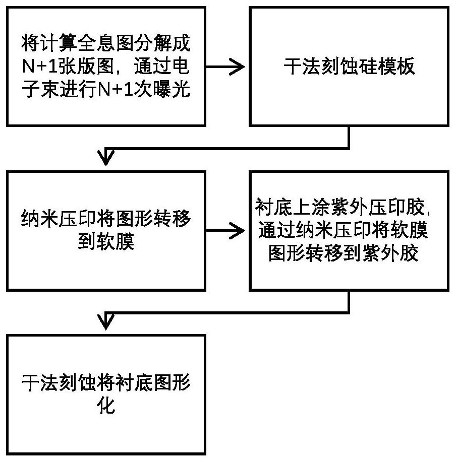
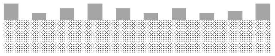
[0035] Such as figure 1 As shown, this embodiment provides a method for preparing a spatial light filter with a 2.5D micro-nano structure by electron beam grayscale exposure, including the following steps:

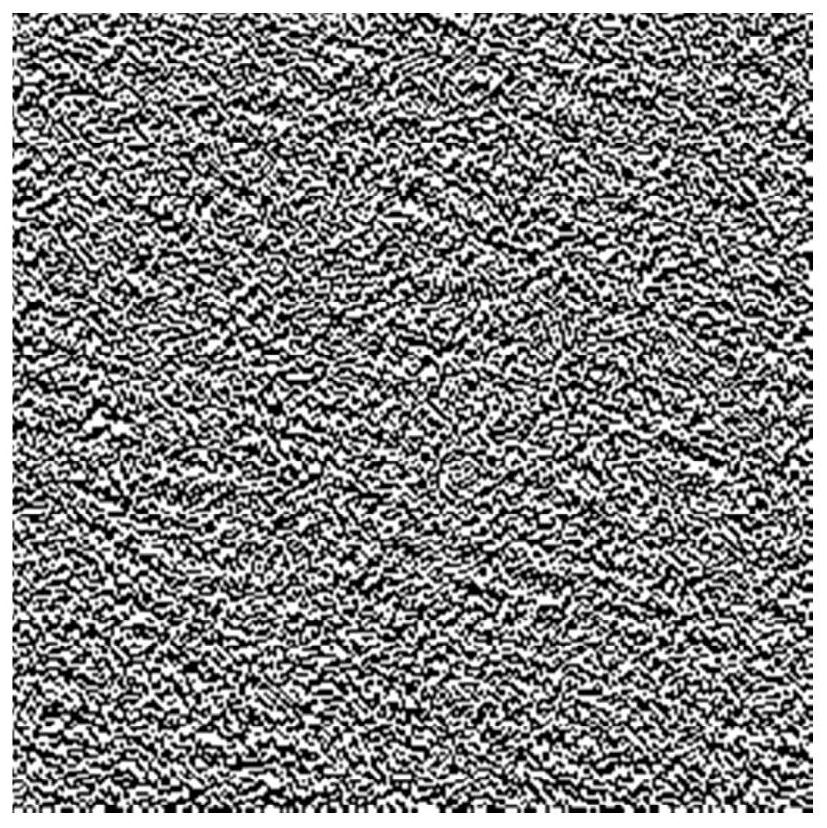
[0036] Step 1: Perform Fourier transform on the spectral surface of the object light wave, calculate the amplitude and phase through the Gauss-Seidel iterative method, assign the amplitude to 0, retain the phase, iterate 100 times, and optimize to obtain a pure phase hologram . Divide the phase of each pixel of the hologram into 2 to the 5th power, that is, 32 levels, divide by 2 in turn to get the remainder, and establish 5 layouts, one of which is shown in Figure 2(a), and then calculate the Union to create an additional compensation layout. 6 e-beam exposures after spin-coating e-beam photoresist on silicon wafers;

[0037] Among them, the exposure beam current of the compensation pattern is 20hA, and the dose is 164μC / cm 2 , the beam currents of the electron beam e...

Embodiment 2

[0054] This embodiment provides a method for preparing a spatial light filter with a 2.5D micro-nano structure by gray-scale exposure of ultraviolet overcoating, including the following steps:

[0055] Step 1: Perform Fourier transform on the spectrum surface of the object light wave, discard the amplitude through the Gauss-Seidel iteration method, iterate 100 times, and optimize to obtain a pure phase hologram. Divide the phase of each pixel of the hologram into 2 to the 5th power, that is, 32 levels, divide by 2 in turn to get the remainder, and establish 5 layouts, and then find the union of these 5 layouts to create an additional compensation layout. After spin-coating AZ5214 UV photoresist on the silicon wafer, perform 6 UV mask overlay alignment exposures;

[0056] Among them, the exposure dose of the compensation pattern is 32mJ / cm 2 , the UV exposure doses of the remaining 5 layouts were 2mJ / cm 2 , 4mJ / cm 2 , 8mJ / cm 2 、16mJ / cm 2 and 32mJ / cm 2 ;

[0057] After th...


PUM


Abstract

The invention discloses a method for preparing a 2.5 D micro-nano structure through gray exposure, and belongs to the technical field of microstructures in semiconducting science. The method comprises the steps of: dividing the height of the 2.5 D micro-nano structure into 2N levels, establishing corresponding N binary exposure layouts, wherein N is larger than I; acquiring a union set of the N binary exposure layouts, and establishing an additional compensation layout; carrying out N+1 times of layered exposure after spin-coating photoresist on the silicon wafer to obtain a photoresist layer containing 2N heights; and using the photoresist layer as a mask to perform dry etching to prepare a nanoimprint template, and realizing batch production through soft film thermocuring nanoimprint and secondary transfer printing of ultraviolet curing nanoimprint. The nanoimprint template is high in pattern precision and has 2N different heights, and the micro-nano structure prepared through soft film transfer printing, nanoimprint and dry etching is high in efficiency, high in yield and accurate in size.

Description

technical field [0001] The invention belongs to the field of microstructures in semiconductor science, and more specifically relates to a method for preparing 2.5D micro-nano structures by grayscale exposure. Background technique [0002] With the development and progress of semiconductor technology, the precision of microstructure processing has reached the nanometer scale. Among them, laser direct writing, ultraviolet lithography, electron beam exposure and nanoimprinting can all produce grayscale exposure patterns. However, the large-area preparation of 2.5D micro-nano structures (micro-nano structures with different height levels) still has problems such as high cost and difficult fabrication. [0003] Taking the spatial light filter as an example, the current 2.5D imprint template is generally prepared by maskless laser direct writing and dry etching technology, but the laser direct writing grayscale exposure has problems such as large stitching error of the writing fi...

Claims


Application Information

Patent Timeline
Patent Type & Authority Applications(China)
IPC IPC(8): B81C1/00G03F7/00
CPCB81C1/00444B81C1/0046B81C1/00531G03F7/0002
Inventor 李攀卢宏夏金松李宇航曾成郑盼盼
Owner HUAZHONG UNIV OF SCI & TECH
Why Eureka
Try Eureka