
JBS (Junction Barrier Schottky) diode

A junction barrier Schottky and diode technology, applied in the field of diodes, can solve the problems of large reverse leakage current and low reverse bias voltage of Schottky diodes, and achieve the effect of improving withstand voltage performance and improving effect.

Active Publication Date: 2017-05-31
南通旺峰电子科技有限公司
View PDF4 Cites 3 Cited by
  • Summary
  • Abstract
  • Description
  • Claims
  • Application Information

AI Technical Summary

Problems solved by technology

[0004] However, Schottky diodes have low reverse bias voltage and large reverse leakage current

Method used


Image

  • JBS (Junction Barrier Schottky) diode
  • JBS (Junction Barrier Schottky) diode

Examples


no. 1 example

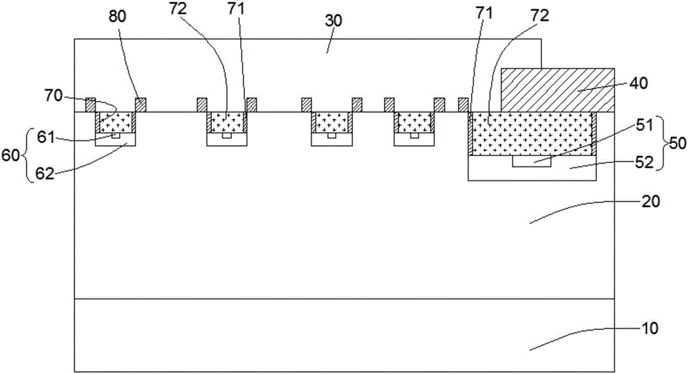
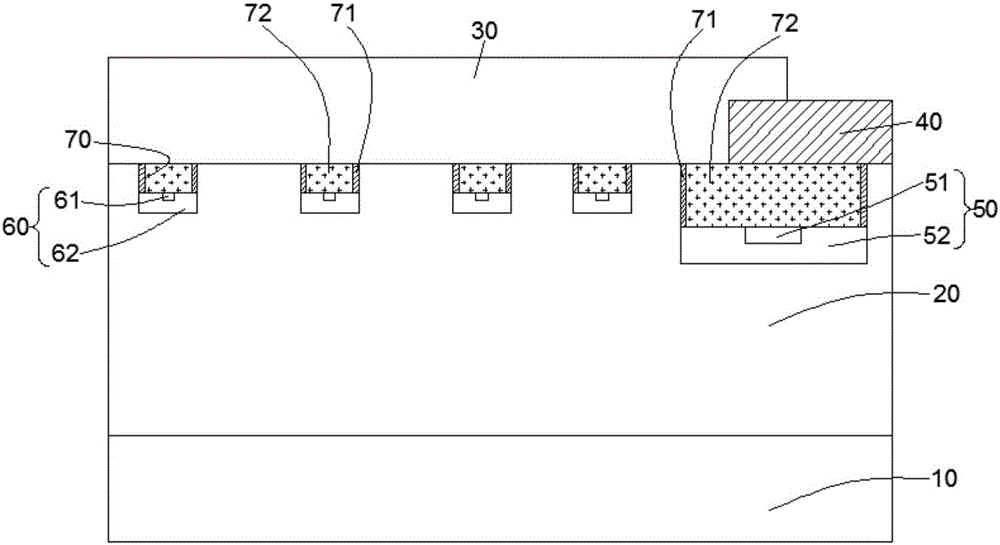
[0025] like figure 1 As shown, a junction barrier Schottky diode includes: a first conductivity type substrate 10, a first conductivity type semiconductor layer 20 formed on the first conductivity type substrate 10, and a first conductivity type semiconductor layer 20 formed on the first conductivity type substrate An anode metal layer 30 on the conductivity type semiconductor layer 20 and forming a Schottky contact with it, an insulating layer 40 formed on the first conductivity type semiconductor layer 20 from the edge of the anode metal layer 30 to the outer side, formed on the insulation layer 30 Layer 40 and the terminal protection area 50 of the second conductivity type under the anode metal layer 30, forming a plurality of second conductivity type semiconductor layers with a certain interval in the upper surface layer of the first conductivity type semiconductor layer 20 inside the terminal protection area 50 The semiconductor region 60, a plurality of trenches 70 with ...

no. 2 example

[0033] In this embodiment, compared with the first embodiment, the groove between the first conductivity type semiconductor layer 20 and the anode metal layer 30 and the groove above the second conductivity type semiconductor region 60 outside the notch of the groove 70 above the terminal protection region 50 The insulating dielectric region 80 is formed between the first conductivity type semiconductor layer 20 outside the notch of the trench 70 and the anode metal layer 30 to prevent the contact between the first conductivity type semiconductor layer 20 at the notch of the trench 70 and the anode metal layer 30 from causing tip discharge to increase leakage current.


PUM


Abstract

The invention relates to the technical field of semiconductors, in particular to a JBS (Junction Barrier Schottky)-structured diode. The JBS diode comprises a first conductive type substrate, a first conductive type semiconductor layer, an anode metal layer, an insulating layer, a terminal protection region and a second conductive type semiconductor region, wherein multiple grooves are formed in the upper surface layer of the first conductive type semiconductor layer at certain intervals; the terminal protection region and the second conductive type semiconductor region are formed below the grooves; insulated side walls are formed on side walls of the grooves; the grooves are filled with conductive materials. According to the JBS diode, the improvement function of a PN junction of the JBS diode on voltage withstanding performance of the diode is effectively improved.

Description

technical field [0001] The invention relates to the technical field of semiconductors, in particular to a diode with a junction barrier Schottky structure. [0002] technical background [0003] A Schottky diode is a semiconductor element that connects a semiconductor layer and a metal layer through a Schottky junction, and utilizes a Schottky barrier to rectify. Schottky diodes can work faster than ordinary PN junction diodes, and have the characteristics of small forward voltage drop. They are mostly used as high-frequency, low-voltage, high-current rectifier diodes, freewheeling diodes, and protection diodes. They are also useful in microwave Used as rectifier diodes and small-signal detector diodes in communications and other circuits, it is more common in communication power supplies, frequency converters, etc. [0004] However, Schottky diodes have low reverse bias voltage and large reverse leakage current. A junction barrier Schottky (JBS) structure diode is a combin...

Claims


Application Information

Patent Timeline
IPC IPC(8): H01L29/872H01L29/06
Inventor 李风浪
Owner 南通旺峰电子科技有限公司
Learn More