Uni-traveling-carrier photodetector structure and manufacturing method thereof

A single-row carrier and photodetector technology, used in semiconductor devices, final product manufacturing, sustainable manufacturing/processing, etc., can solve problems such as increasing the RC response bandwidth of devices, and achieve a controllable and large collection layer area reduction. Responsiveness, effect of large RC response bandwidth

Active Publication Date: 2017-05-31
SHANGHAI INST OF MICROSYSTEM & INFORMATION TECH CHINESE ACAD OF SCI
View PDF5 Cites 5 Cited by
  • Summary
  • Abstract
  • Description
  • Claims
  • Application Information

AI Technical Summary

Problems solved by technology

[0007] In view of the above-mentioned shortcomings of the prior art, the purpose of the present invention is to provide a single-line carrier photodetector structure and its manufacturing method, which is used to solve the problem that the existing UTC-PD cannot improve the high incident light power of the device and The problem of increasing the RC response bandwidth of the device while increasing the photoresponsivity

Method used


Image

  • Uni-traveling-carrier photodetector structure and manufacturing method thereof
  • Uni-traveling-carrier photodetector structure and manufacturing method thereof
  • Uni-traveling-carrier photodetector structure and manufacturing method thereof

Examples


Embodiment 1

[0058] This embodiment provides a method for manufacturing a single row carrier photodetector, the method comprising:

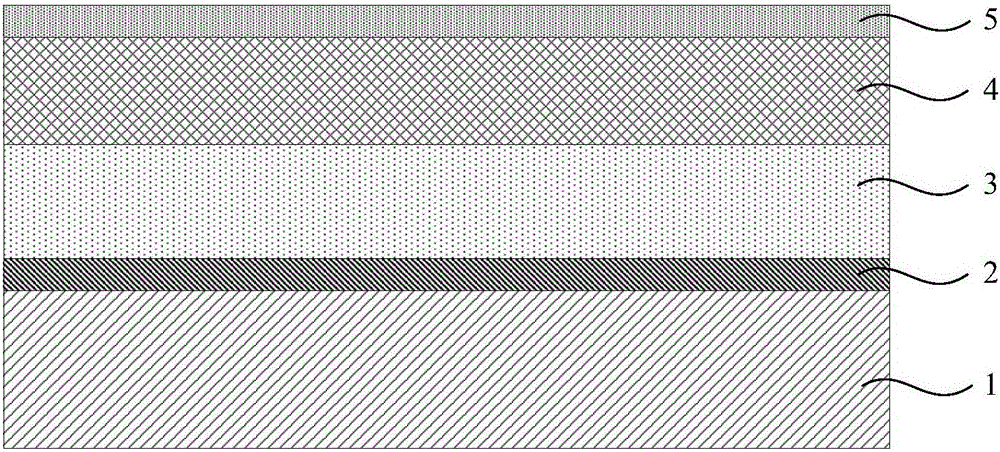
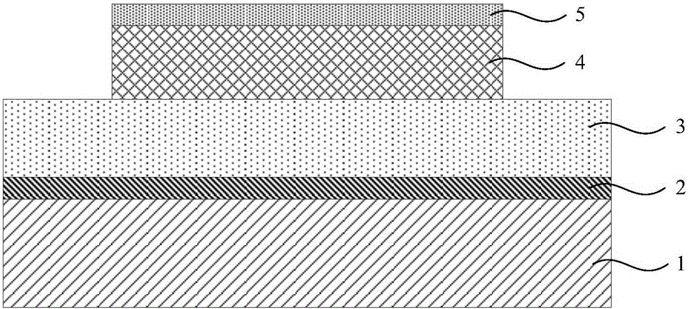
[0059] S1: growing an N-type heavily doped lower contact layer, a collection layer, an absorber layer, and a P-type heavily doped upper contact layer sequentially from bottom to top on a semi-insulating substrate;

[0060] S2: performing photolithography on the structure described in S1, and using a selective etching solution to etch the P-type heavily doped upper contact layer and the absorber layer to expose part of the collection layer;

[0061] S3: growing a silicon nitride layer on the upper surface of the structure described in S2, and removing the silicon nitride layer on the upper surface of the collection layer by photolithography;

[0062] S4: Using a selective etching solution to etch the collection layer so that the area of ​​the collection layer is equal to the area of ​​the absorption layer, and then continue to corrode the collection layer unti...

Embodiment 2

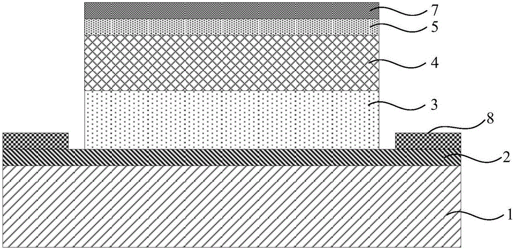
[0085] Such as Figure 9 with Figure 10 As shown, this embodiment provides a single row carrier photodetector structure, and the photodetector structure includes:

[0086] semi-insulating substrate 1;

[0087] An N-type heavily doped lower contact layer 2 located on the upper surface of the semi-insulating substrate 1;

[0088] A collection layer 3 located on the upper surface of the N-type heavily doped lower contact layer 2;

[0089] The lower electrode metal layer 8 located on the upper surface of the N-type heavily doped lower contact layer 2 and on both sides of the collection layer 3;

[0090] An absorbing layer 4 located on the upper surface of the collecting layer 3;

[0091] a P-type heavily doped upper contact layer 5 located on the upper surface of the absorber layer 4; and

[0092] The upper electrode metal layer 7 located on the upper surface of the P-type heavily doped upper contact layer 5;

[0093] Wherein, the area of ​​the collecting layer 3 is smaller...

Embodiment 3

[0098] This embodiment provides a method for manufacturing a single row carrier photodetector, the method comprising:

[0099] S1: Grow a waveguide layer, N-type heavily doped lower contact layer, collection layer, absorber layer, and P-type heavily doped upper contact layer sequentially from bottom to top on a semi-insulating substrate;

[0100] S2: performing photolithography on the structure described in S1, and using a selective etching solution to etch the P-type heavily doped upper contact layer and the absorber layer to expose part of the collection layer;

[0101] S3: growing a silicon nitride layer on the upper surface of the structure described in S2, and removing the silicon nitride layer on the upper surface of the collection layer by photolithography;

[0102] S4: Using a selective etching solution to etch the collection layer so that the area of ​​the collection layer is equal to the area of ​​the absorption layer, and then continue to corrode the collection laye...


PUM


Abstract

The invention provides a uni-traveling-carrier photodetector structure and a manufacturing method thereof. A photodetector structure with a collection layer area smaller than an absorption layer area is manufactured by utilizing a stepwise corrosion method, so that device capacitance is greatly reduced, the RC response bandwidth of a device is increased under the condition of the same absorption layer thickness, and the total bandwidth of the device is increased; the device has a larger absorption layer area under the condition of the same absorption layer area and the same absorption layer thickness (the RC bandwidth and the transition bandwidth are same), so that the device has a higher response degree and can work under higher incident power, and the performance improvement is more remarkable in high-speed high-power application; and therefore, the photodetector structure is suitable for the fields of terahertz signal generation, light receiving in high-speed light communication, and the like.

Description

technical field [0001] The invention belongs to the technical field of semiconductor optoelectronic devices, and in particular relates to a single row carrier photodetector structure and a manufacturing method thereof. Background technique [0002] The terahertz (hereinafter referred to as THz, 1THz=1012Hz) band refers to the frequency in the electromagnetic spectrum from 100 GHz to 10 THz, the corresponding wavelength is from 3 mm to 30 microns, and the area of ​​the electromagnetic spectrum between millimeter waves and infrared light. There are broad application prospects in security imaging and other aspects. Among them, THz wireless communication can meet the bandwidth demand of future wireless high-speed data transmission. The method of using optical mixing to generate THz radiation inherits the advantages of photonics technology. It has the characteristics of continuous output, broadband tunable, high output power, normal temperature operation, and high cost performanc...

Claims


Application Information

Patent Timeline
Patent Type & Authority Applications(China)
IPC IPC(8): H01L31/18H01L31/102H01L31/109H01L31/0352
CPCH01L31/035272H01L31/035281H01L31/102H01L31/109H01L31/1844Y02P70/50
Inventor 姚辰张戎曹俊诚
Owner SHANGHAI INST OF MICROSYSTEM & INFORMATION TECH CHINESE ACAD OF SCI
Why Eureka
Try Eureka