Light-emitting device, display device and lighting device containing light-emitting device, and solar cell

A technology for solar cells and light-emitting devices, applied in the optical field, can solve problems such as unbalanced injection of holes and electrons, and achieve the effects of solving the unbalanced injection of holes and electrons, improving mobility, and improving luminous efficiency.

Active Publication Date: 2017-05-31
NANJING TECH CORP LTD
View PDF3 Cites 10 Cited by
  • Summary
  • Abstract
  • Description
  • Claims
  • Application Information

AI Technical Summary

Problems solved by technology

[0005] The main purpose of the present invention is to provide a light-emitting device, a display device containing it, a lighting device, and a solar cell, so as to solve the problem of unbalanced injection of holes and electrons in the prior art

Method used


Image

  • Light-emitting device, display device and lighting device containing light-emitting device, and solar cell
  • Light-emitting device, display device and lighting device containing light-emitting device, and solar cell
  • Light-emitting device, display device and lighting device containing light-emitting device, and solar cell

Examples


preparation example Construction

[0054] In another embodiment of the present application, a method for preparing an organic polymer hole transport material-metal sulfide is provided, the preparation method comprising:

[0055] Step S1, reacting dodecanoic acid, concentrated sulfuric acid and organic polymer hole transport material in a solvent of cyclohexane and dimethylformamide at 45-55°C for 2 hours to obtain an initial reaction solution; step S2, making the initial The reaction solution reacts with the metal chloride corresponding to the metal sulfide at 65-75° C. for 2 hours to obtain an organic polymer hole transport material-metal sulfide solution.

[0056] In the above-mentioned embodiments, chemical methods are mainly used to connect the organic polymer hole transport material and the deep energy level material by covalent bonds. Taking the synthesis of PVK-CdS nanoparticles as an example, it is mainly through the side of the S atom. It is formed by connecting the C atom on the benzene ring in PVK an...

Embodiment 1

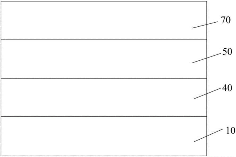
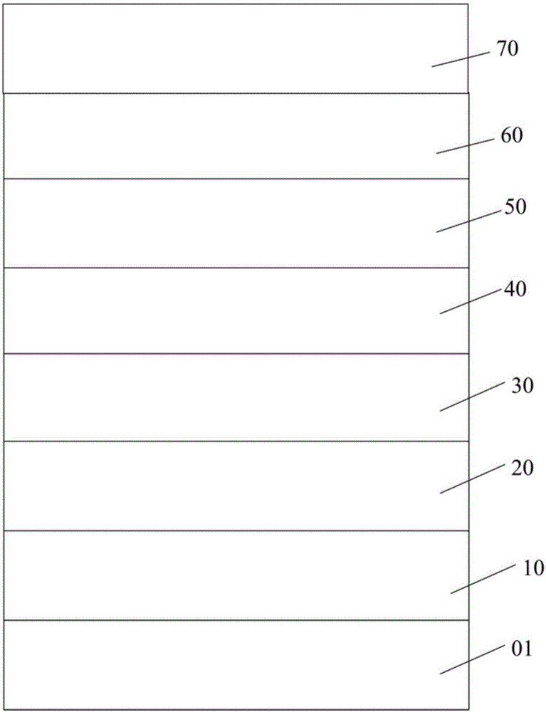
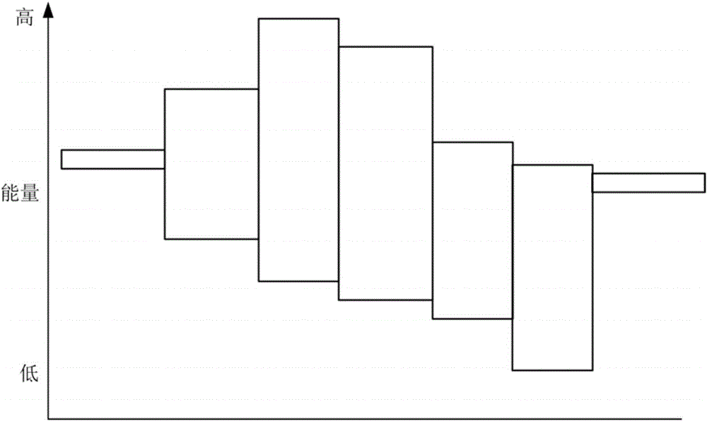
[0066] The structure of the light-emitting device is as follows: the substrate 01 is a glass substrate, the material of the anode layer 10 is ITO, and the thickness is 150nm. The second hole transport layer is set on the surface of the hole injection layer away from the anode layer 10. The material is PVK with a thickness of 30nm. The material of the first hole transport layer 40 is PVK-CdS nanoparticles with a thickness of 5nm. The luminescent material of the layer 50 is CdSe / CdS red core-shell quantum dots, the wavelength range of its absorption spectrum is between 300-610nm, the thickness of the luminescent layer 50 is 20nm; the material of the cathode layer 70 is Ag, the thickness is 100nm, electron transmission Layer, arranged between the second hole transport layer and the light-emitting layer, its material includes ZnO, the thickness is 40nm; wherein, the HOMO energy level of the metal sulfide CdS is -6.8eV; the HOMO of the organic polymer hole transport material PVK Th...

Embodiment 2

[0069] The difference between the light-emitting device provided in this example and Example 1 is that the metal sulfide is ZnS, and ZnCl with a mass of 0.0273g 2 Instead of CdCl in Example 1 2 , the HOMO energy level of ZnS as the metal sulfide is -7eV, and the HOMO energy level of the nanoparticles in the first hole transport layer is -6.3eV.


PUM


Abstract

The invention provides a light-emitting device, a display device and lighting device containing the light-emitting device and a solar cell. The light-emitting device comprises an anode layer, a first hole transport layer, a light-emitting layer and a cathode layer, wherein the first hole transport layer is arranged on the surface of the anode layer, and a material for forming the first hole transport layer comprises nanoparticles; the nanoparticles are organic polymer hole transport material-metal sulfide; an organic polymer hole transport material is connected with metal sulfide through a covalent bond; the highest occupied molecular orbital energy level of the metal sulfide is deeper than that of the organic polymer hole transport material; the light-emitting layer is arranged on the surface, far away from the anode layer, of the first hole transport layer, and the material for forming the light-emitting layer comprises a light-emitting material; and the cathode layer is arranged on the surface, far away from the first hole transport layer, of the light-emitting layer. The rates that electrons and holes in the light-emitting device are injected into the light-emitting layer are basically consistent, so that the electrons and the holes approach or reach injection balance, the light-emitting efficiency of the device is improved and the service life of the device is prolonged.

Description

technical field [0001] The invention relates to the field of optical technology, in particular to a light emitting device, a display device and an illuminating device containing the same, and a solar cell. Background technique [0002] In the current typical light-emitting devices, due to the energy level between the highest occupied orbital of the commonly used organic polymer hole transport layer (the orbital with the highest energy level of occupied electrons, HOMO for short) and the valence band energy of the light-emitting material of the light-emitting layer The relatively large level difference makes it difficult for holes to be injected into the light-emitting layer, which leads to an unbalanced injection of holes and electrons, which affects the efficiency of the light-emitting device. [0003] In the prior art, a hole transport layer is generally provided between the anode layer and the light-emitting layer to reduce the barrier of hole transport, but the function ...

Claims


Application Information

Patent Timeline
Patent Type & Authority Applications(China)
IPC IPC(8): H01L51/50H01L51/54
CPCH10K50/11H10K2101/40H10K50/156H10K50/15
Inventor 陈涛
Owner NANJING TECH CORP LTD
Why Eureka
Try Eureka