

Method for realizing Si-Si bonding through adoption of amorphous germanium film
An amorphous germanium and thin film technology, applied in the field of low-temperature Si-Si bonding, can solve the problems that the interface cannot be crystallized and cannot meet the needs of large-scale integrated circuits, and achieves the effect of simple cost, avoiding incompatibility and low cost
- Summary
- Abstract
- Description
- Claims
- Application Information
AI Technical Summary
Problems solved by technology
Method used
Image

Examples
Embodiment Construction
[0031] The following embodiments will further illustrate the present invention in conjunction with the accompanying drawings.
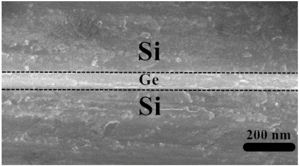
[0032] The equipment used is a TRP-450 composite film sputtering deposition system, and two DC targets and one RF target are placed in the growth chamber. The target material used is a high-purity Ge circular target material of 5N (above 99.999%). The used Si substrate material is a (100) N-type single crystal Si wafer, polished on one side, and has a resistivity of 1-5Ω·m.
[0033] 1. The processing of Si substrate material, the specific method is as follows:
[0034] 1) Select a Si substrate material with a crystal orientation of (100), and ultrasonically clean it with acetone and ethanol for 10 minutes respectively to remove organic matter on the surface of the substrate.
[0035] 2) The Si wafer after the organic ultrasonic cleaning was first washed with H 2 SO 4 :H 2 o 2 = 4:1 mixed solution boiled for 10min, then HF:H 2 o 2 = Soak in the...
PUM
| Property | Measurement | Unit |
|---|---|---|
| electrical resistivity | aaaaa | aaaaa |
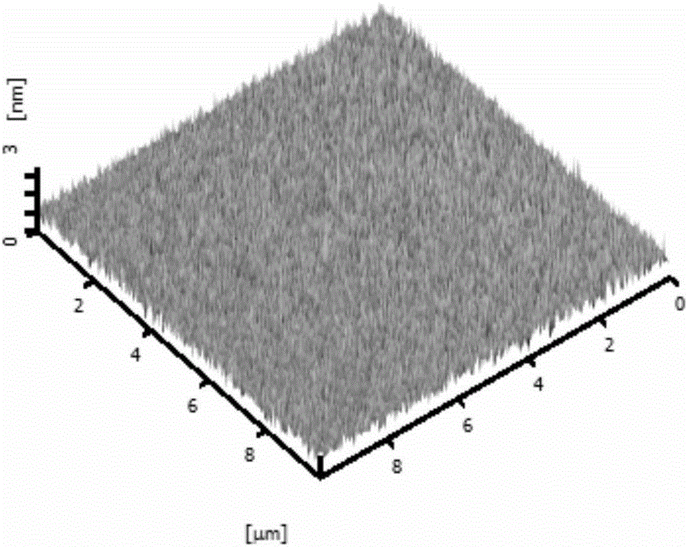
| surface roughness | aaaaa | aaaaa |
Abstract
Description
Claims
Application Information