
A Method for Realizing Low Temperature Si-Si Bonding Using Amorphous Germanium Thin Films

An amorphous germanium and si-si technology, which is applied in the field of low-temperature Si-Si bonding, can solve the problems that the interface cannot be crystallized and cannot meet the needs of large-scale integrated circuits, and achieve simple cost, avoid incompatibility, and low cost. Effect

Inactive Publication Date: 2019-04-12
XIAMEN UNIV
View PDF5 Cites 0 Cited by
  • Summary
  • Abstract
  • Description
  • Claims
  • Application Information

AI Technical Summary

Problems solved by technology

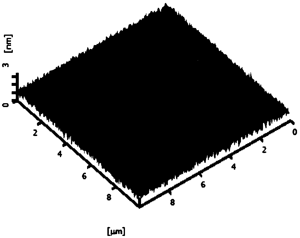
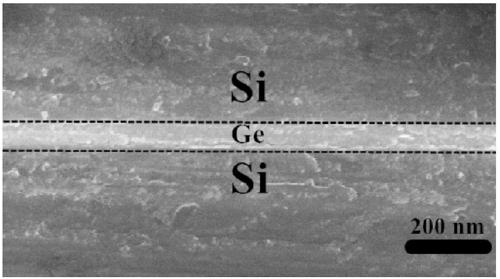
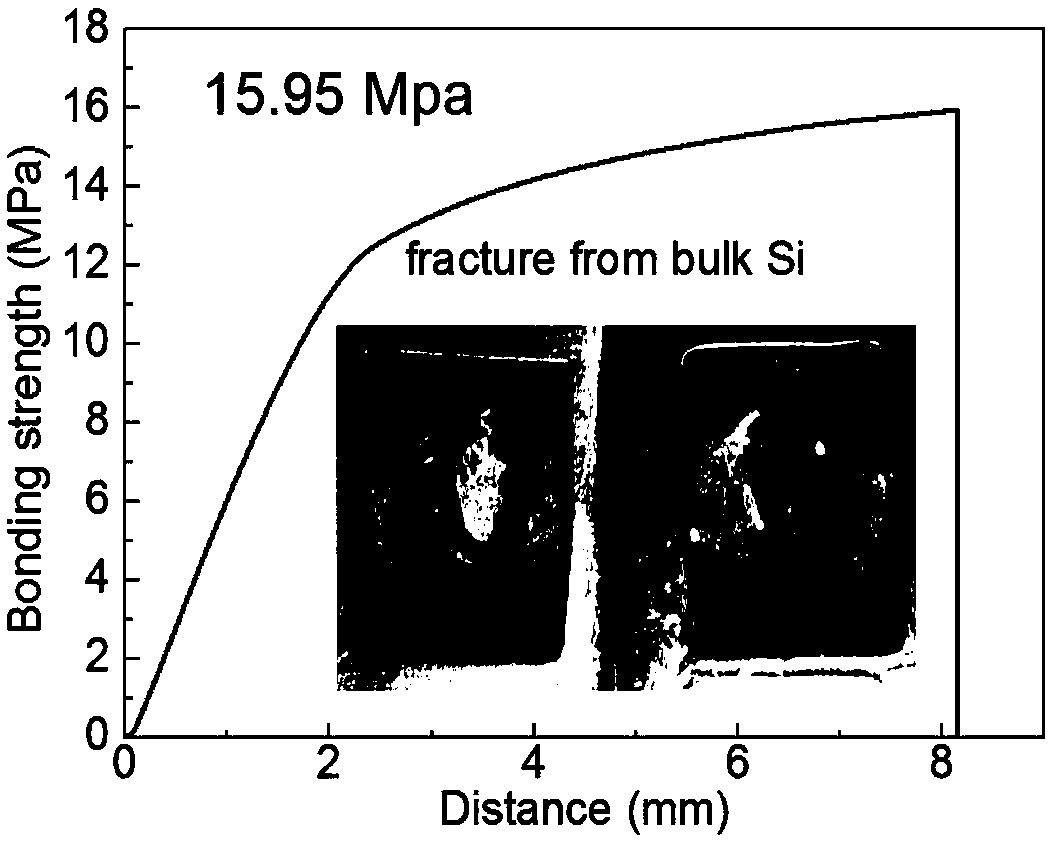
[0004] The purpose of the present invention is to solve the problem that high-temperature Si-Si direct bonding cannot meet the requirements of large-scale integrated circuits and the low-temperature bonding interface cannot be crystallized by using an a-Si interlayer, and provides a method for realizing low-temperature Si-Si bonding by using an amorphous germanium film. method

Method used


Image

  • A Method for Realizing Low Temperature Si-Si Bonding Using Amorphous Germanium Thin Films
  • A Method for Realizing Low Temperature Si-Si Bonding Using Amorphous Germanium Thin Films
  • A Method for Realizing Low Temperature Si-Si Bonding Using Amorphous Germanium Thin Films

Examples


Embodiment Construction

[0031] The following embodiments will further illustrate the present invention in conjunction with the accompanying drawings.

[0032] The equipment used is a TRP-450 composite film sputtering deposition system, and two DC targets and one RF target are placed in the growth chamber. The target material used is a high-purity Ge circular target material of 5N (above 99.999%). The used Si substrate material is a (100) N-type single crystal Si wafer, polished on one side, and has a resistivity of 1-5Ω·m.

[0033] 1. The processing of Si substrate material, the specific method is as follows:

[0034] 1) Select a Si substrate material with a crystal orientation of (100), and ultrasonically clean it with acetone and ethanol for 10 minutes respectively to remove organic matter on the surface of the substrate.

[0035] 2) The Si sheet after the organic ultrasonic cleaning was first washed with H 2 SO 4 :H 2 o 2 = 4:1 mixed solution boiled for 10min, then HF:H 2 o 2 = Soak in a m...


PUM

PropertyMeasurementUnit
electrical resistivityaaaaaaaaaa
surface roughnessaaaaaaaaaa

Abstract

The present invention provides a method for realizing Si-Si bonding through adoption of an amorphous germanium film, and relates to a Si wafer bonding method. The method comprises: selecting Si substrate materials with crystal direction as (100), performing cleaning; boiling the substrate materials through adoption of a mixed solution of H2SO4 and H2O2, and immersing the substrate materials in a mixed solution of HF and H2O2; boiling the processed Si wafer in a mixed solution of NH4OH, H2O2 and H2O, and immersing Si wafer in a mixed solution of HF and H2O2; boiling the processed Si wafer in a mixed solution of HCL, H2O2 and H2O, and immersing the Si wafer in a mixed solution of HF and H2O2; drying the processed Si wafer to put the Si wafer into a direct current magnetron sputtering system, filling Ar gas into a sputtering chamber when the base pressure of the sputtering chamber is smaller than 1*10<-4>Pa; sputtering a-Ge thin film through regulation of direct current sputtering current and sample holder rotation speed; and realizing high-intensity Si-Si bonding through adoption of a hydrophilic a-Ge layer.

Description

technical field [0001] The invention relates to a Si wafer bonding method, in particular to a method for realizing low-temperature Si-Si bonding by using an amorphous germanium film. Background technique [0002] As a basic process in the field of microelectronics, Si-Si direct bonding has attracted more and more attention. Si-Si direct bonding is a technology that realizes wafer integration by cleaning, activating, bonding at room temperature, and heat treatment at high temperature for two polished Si wafers ([1] Howlader M M R, Wang J G, Kim M J .Influence of nitrogenmicrowave radicals on sequential plasma activated bonding[J].MaterialsLetters,2010,64(3):445-448;[2]Toyoda E,Sakai A,Isogai H,et al.Mechanical Properties and Chemical Reactions at the Directly Bonded Si–Si Interface [J]. Japanese Journal of Applied Physics, 2009, 48(1R): 011202.), although the bonding technology started relatively late, but developed very rapidly, its principles, methods and experimental equi...

Claims


Application Information

Patent Timeline
Patent Type & Authority Patents(China)
IPC IPC(8): H01L21/20H01L21/60C23C14/16C23C14/35
CPCC23C14/165C23C14/35H01L21/20H01L24/03
Inventor 陈松岩柯少颖林绍铭李成黄巍
Owner XIAMEN UNIV
Learn More