

Preparation method of drain electrode lightly-offset structure
A drain and gate layer technology, applied in semiconductor/solid-state device manufacturing, electrical components, circuits, etc., can solve problems such as repeatability, poor uniformity, lower product reliability, and poor slope angle, and achieve easy control of dimensions , Improve reliability, reduce the effect of leakage current
- Summary
- Abstract
- Description
- Claims
- Application Information
AI Technical Summary
Problems solved by technology
Method used
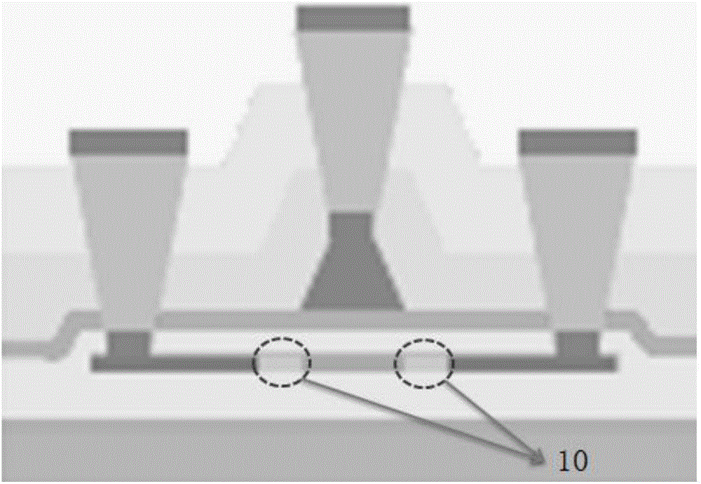
Image

Examples
Embodiment Construction
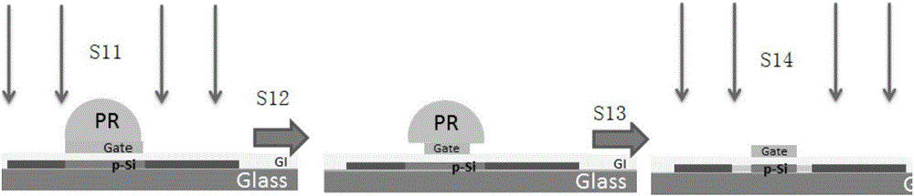
[0029] The implementation of the present invention will be described in detail below in conjunction with the accompanying drawings. The accompanying drawings are only for reference and description, and do not constitute a limitation to the protection scope of the present invention.
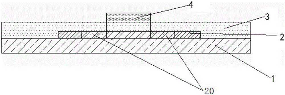
[0030] see Figure 4 , Figure 5 , the embodiment of the present invention provides a method for preparing a light drain offset LDO structure, including the steps of crystallization of the glass substrate Glass1, imaging of the P-Si substrate 2, film formation of the gate insulating layer GI3 and film formation of the gate layer Gate4, The drain light offset LDO structure is formed by the following steps:
[0031] S1. Coating step: coating photoresist PR5 on the gate layer Gate4;
[0032] S2. Half-tone exposure step: exposing the photoresist layer PR5 through a half-tone mask Half-tone Mask6;
[0033] S3. Developing step: developing the photoresist layer PR5 after halftone exposure;
[0034] S...
PUM
 Abstract
Description
Claims
Application Information