

A kind of preparation method of lateral graphene pin junction
A graphene, lateral technology, applied in semiconductor/solid-state device manufacturing, electrical components, circuits, etc., can solve problems such as difficulty in realizing graphene PIN junctions, and achieve the effects of easy implementation, simple process, and improved performance
- Summary
- Abstract
- Description
- Claims
- Application Information
AI Technical Summary
Problems solved by technology
Method used
Image

Examples
Embodiment 1
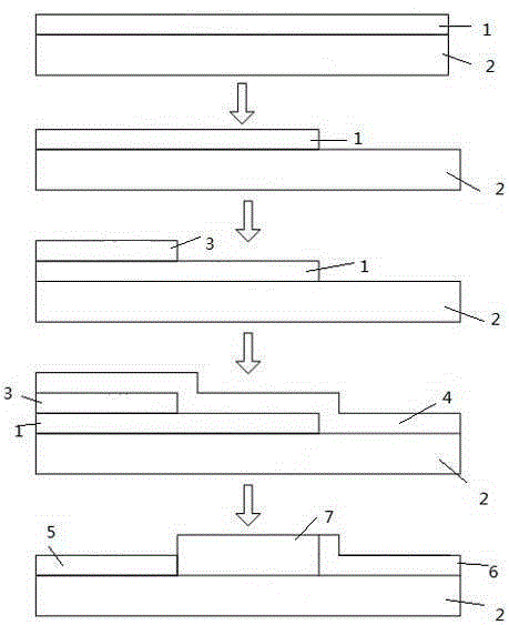
[0020] Depend on figure 1 As can be seen from the shown flow chart, the preparation steps of Example 1 are:
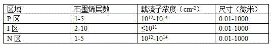
[0021] In the first step, the underlying graphene is grown on the SiC substrate 2 by SiC pyrolysis, the doping type of the underlying graphene is n-type, and the doping concentration is 10 12 -10 14 cm -2 controllable.
[0022] In the second step, photolithography is used to retain the region that needs to retain n-type doping on the bottom graphene, and other regions are removed by oxygen plasma etching; the region that needs to retain n-type doping is to be used as N region 5 and I region 7, the removed area is the area to be used as the P area 6.
[0023] The third step is to precipitate Si on the bottom graphene in the sample obtained in the second step above, which needs to be an n-type region 3 N 4 Blocking layer 3.
[0024] The fourth step is to transfer the p-type transfer graphene 4 grown by CVD to the sample obtained in the third step. At this time, t...
Embodiment 2
[0028] Different from Example 1, the preparation steps of Example 2 are:
[0029] In the first step, the n-type bottom graphene 1 is grown on the SiC substrate 2 by the CVD method, and the bottom graphene is annealed in a hydrogen atmosphere, and the hydrogen atoms enter the interface between the bottom graphene and the SiC substrate 2, so that the bottom graphene Converted to p-type doping with a doping concentration of 10 12 -10 14 cm -2 controllable.
[0030] In the second step, photolithography is used to retain the region on the bottom graphene that needs to retain p-type doping, and other regions are removed by oxygen plasma etching; the region that needs to retain p-type doping is to be used as P region 6 and I region 7, the removed area is the area to be used as the N area 5.
[0031] In the third step, SiO is deposited on the region that needs to be p-type in the above-mentioned bottom graphene 2 Occlusion layer.
[0032] The fourth step is to transfer the n-ty...
Embodiment 3
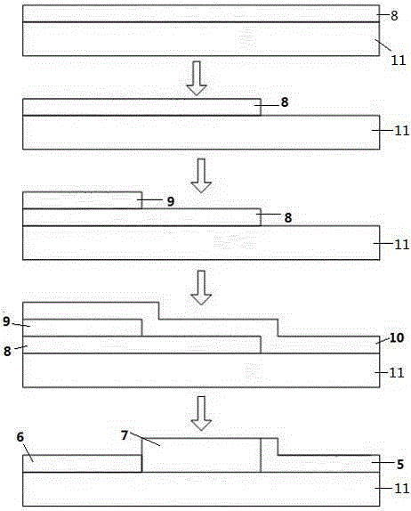
[0036] Depend on figure 2 It can be seen that, unlike Example 1 and Example 2, the specific preparation steps of this example are:
[0037] In the first step, the p-type bottom graphene 8 is grown on the Cu substrate by the CVD method; the p-type bottom graphene 8 is transferred to the Si substrate 11 with a doping concentration of 10 12 -10 14 cm -2 controllable.
[0038] In the second step, photolithography is used to retain the region on the bottom graphene that needs to be retained, and other regions are removed by oxygen plasma etching; the region that needs to retain p-type doping is to be used as P region 6 and I region 7 The area to be removed is the area to be used as the N area 5.
[0039] In the third step, an Au shielding layer 9 is deposited on the region of the bottom graphene that needs to be p-type.
[0040] The fourth step is to transfer the n-type graphene grown by CVD to the sample obtained in the third step. At this time, the surfaces of the shieldin...
PUM
 Abstract
Description
Claims
Application Information