Fabrication method of impurity band detector based on soi blocking

A technology that blocks impurities and detectors. It is applied in semiconductor devices, final product manufacturing, and sustainable manufacturing/processing. It can solve the problems of limiting the quantum efficiency and responsivity of devices, the inability to effectively suppress dark current, and the introduction of impurities. Avoid the low resistivity of the barrier layer, solve the limited thickness of the absorbing layer, and suppress the effect of dark current

CN104576832BActive Publication Date: 2017-01-11NO 50 RES INST OF CHINA ELECTRONICS TECH GRP
2 Cites 0 Cited by

Patent Information

Authority / Receiving Office
CN · China
Patent Type
Patents(China)
Current Assignee / Owner
Publication Date
2017-01-11

Smart Images

  • Figure 1
    Figure 1
  • Figure 2
    Figure 2
  • Figure 3
    Figure 3
Patent Text Reader

Abstract

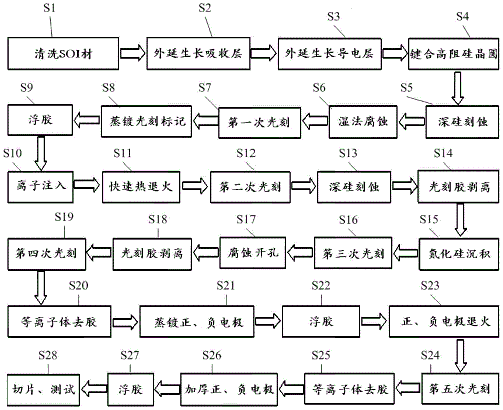
The invention relates to a blocking impurity band detector manufacturing method based on an SOI. The method includes the steps that epitaxial is carried out on a top silicon layer made of SOI materials with an in-situ doping technology to grow an absorbing layer; heavy doping is carried out on the absorbing layer to grow a conducting layer; a high-resistance silicon wafer is bonded to the conducting layer; a bottom silicon layer of the SOI materials is removed with a deep silicon etching technology; a buried oxide layer of the SOI materials is removed with a wet etching technology; an electrode transition area is formed on the top silicon layer of the SOI materials with the ion implantation technology and the rapid thermal annealing technology; a micro-mesa is formed with a deep silicon etching technology, and a silicon nitride passivation layer is deposited; holes are formed in the silicon nitride passivation layer in an etched mode, and positive electrodes and negative electrodes are formed with an electron beam evaporation technology; electrode ohmic contact is formed with an annealing technology; the positive electrodes and the negative electrodes are thickened with an electron beam evaporation technology. According to the technical scheme, the quantum efficiency and the response ratio of a blocking impurity band detector are improved.
Need to check novelty before this filing date? Find Prior Art

Description

technical field

[0001] The invention relates to the preparation technology of infrared and terahertz detection devices, in particular to a preparation method of a detector based on SOI blocking impurity bands. Background technique

[0002] The barrier impurity band detector is a highly sensitive far-infrared and terahertz wave detector, which works in a low temperature environment below 10K, and has broad application prospects in civil, military and aerospace fields. There are mainly the following two fabrication techniques for blocking impurity band detectors. One of them is to epitaxially grow a heavily doped silicon absorber layer on a high-conductivity silicon substrate, and epitaxially grow a high-resistance silicon barrier layer on the absorber layer in the same furnace. The advantage of this preparation method is that the structure and process are relatively simple, and it is easy to increase The disadvantage is that the epitaxially grown high-resistance silicon barr...

Examples

Embodiment Construction

[0036] In order to make the above objects, features and advantages of the present invention more comprehensible, the specific implementation manners of the present invention will be described in detail below in conjunction with the accompanying drawings.

[0037] In the following description, specific details are set forth in order to provide a thorough understanding of the present invention. However, the present invention can be implemented in many other ways than those described here, and those skilled in the art can make similar extensions without departing from the connotation of the present invention. Accordingly, the present invention is not limited to the specific embodiments disclosed below.

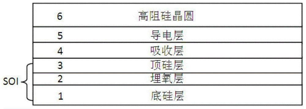
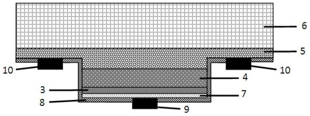
[0038] like figure 1 and figure 2 As shown, the preparation method based on the SOI barrier impurity band detector (hereinafter referred to as the detector) of the present invention is based on the existing mature SOI process technology, and obtains high resistivity through de...