Organic light emitting diode device and manufacturing method thereof

A technology for light-emitting diodes and a manufacturing method, which is applied in the manufacture of semiconductor/solid-state devices, semiconductor devices, electrical components, etc., can solve the problems of film peeling, poor interface adhesion, and inability to bend, so as to block the penetration of gas molecules, improve the Surface adhesion, thickness reduction effect

Inactive Publication Date: 2019-03-12
AAC TECH NANJING
View PDF6 Cites 0 Cited by
  • Summary
  • Abstract
  • Description
  • Claims
  • Application Information

AI Technical Summary

Problems solved by technology

The formed organic light emitting diode device has excellent water and oxygen gas barrier ability, WVTR2 / day, but has the following defects: the thickness is thicker, up to 0.5-0.7mm, the process is more complicated, the high temperature conditions required for the preparation process may have an impact on the cathode of the OLED unit, and the obtained organic light emitting diode device has poor flexibility. feature, inflexible
However, thin-film packaging technology cannot completely solve the problem of water and oxygen penetration. First, because the inorganic thin film is formed by CVD film-forming process, specifically, it is a chemical gas phase reaction triggered by plasma plasma, and active molecules diffuse and adsorb on the substrate to form islands. Forming a continuous film, the process will inevitably produce pinholes and gaps, thereby reducing its water vapor barrier ability; the second is because the organic film has too high a permeability to gas molecules
To solve the problem of water and oxygen permeation in thin-film packaging technology, on the one hand, it is necessary to increase the stacking of the entire thin-film packaging layer to delay the penetration time of gas molecules; on the other hand, it is necessary to increase the thickness of the organic film to further improve product reliability. Only 10-15μm can achieve commercial application effect, which will lead to high production cost and complicated process in the current OLED industry
In addition, in the thin film packaging technology, the inorganic thin film and the organic thin film are two different phases, the interface adhesion is poor, and the thin film is prone to peeling off, which further aggravates the problem of water and oxygen penetration.

Method used


Image

  • Organic light emitting diode device and manufacturing method thereof
  • Organic light emitting diode device and manufacturing method thereof
  • Organic light emitting diode device and manufacturing method thereof

Examples


Embodiment Construction

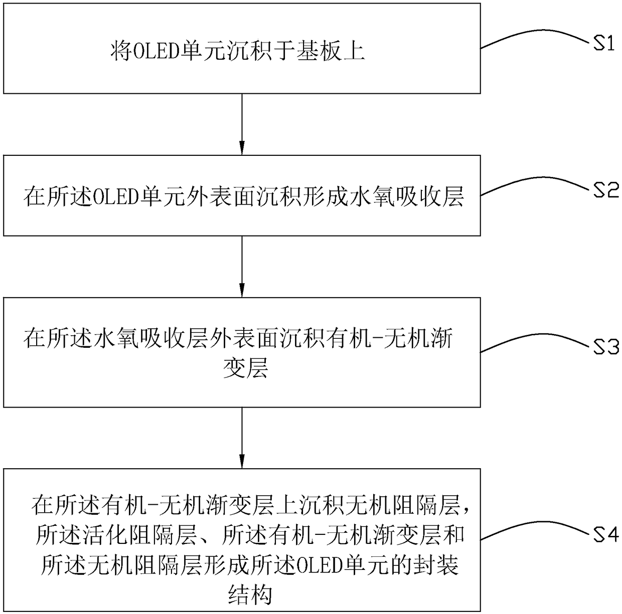
[0030] The present invention will be further described below in conjunction with the accompanying drawings and embodiments.

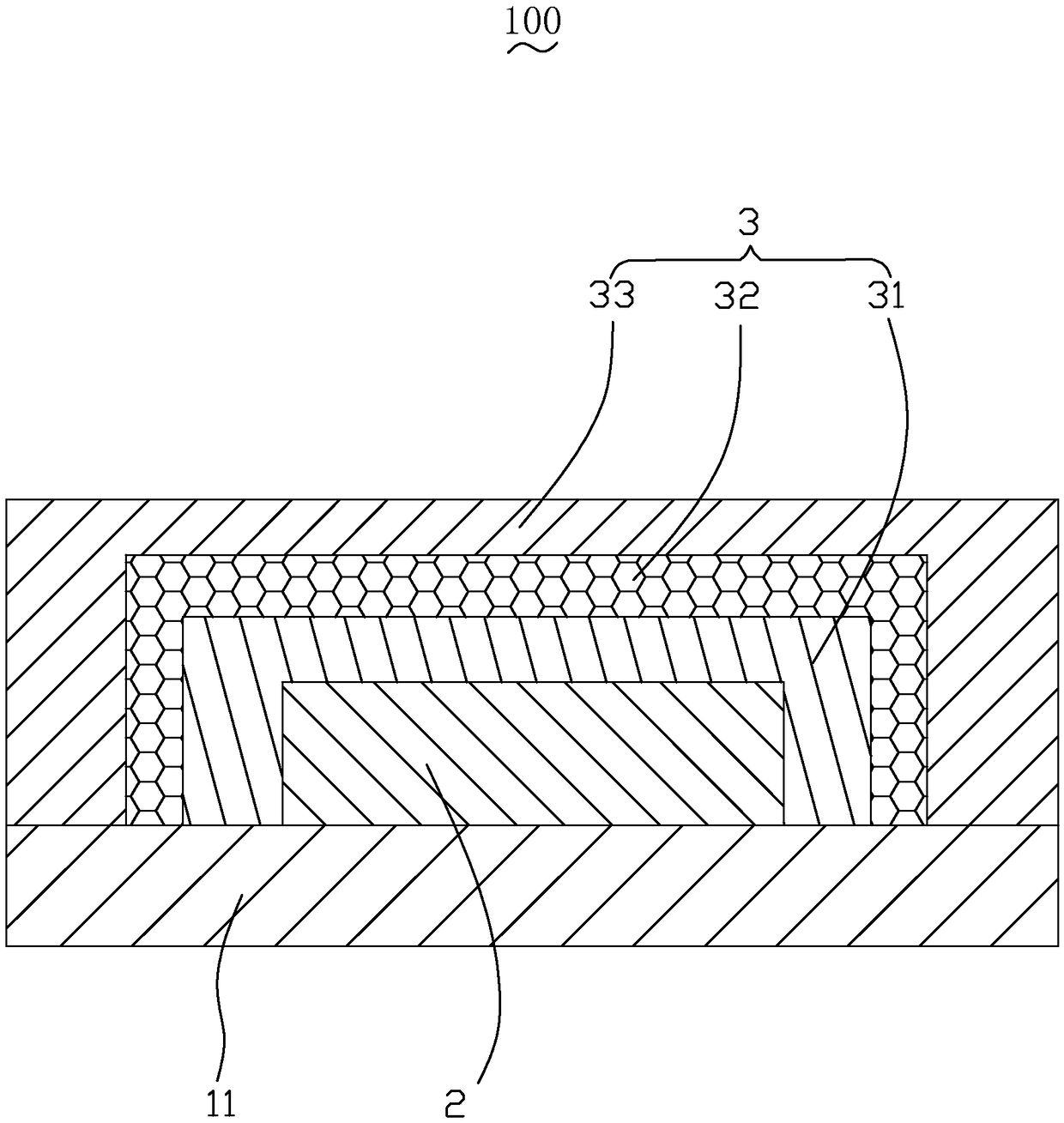
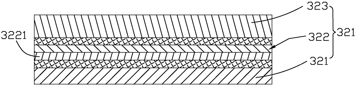
[0031] see figure 1 , is a schematic structural view of the organic light emitting diode device provided by the present invention. The OLED device 100 includes a substrate 1 , an OLED unit 2 disposed on the substrate 1 and an encapsulation structure 3 , the encapsulation structure 3 is connected to the substrate 1 for encapsulating the OLED unit 2 .

[0032] The substrate 1 is a rigid substrate or a flexible substrate, wherein the rigid substrate is glass, silicon wafer or other rigid materials; the flexible substrate is a plastic substrate, aluminum foil, ultra-thin metal or ultra-thin glass.

[0033] The OLED unit 2 includes a conductive anode, a hole transport layer, a light-emitting layer, an electron transport layer and a cathode deposited sequentially, and the cathode is electrically connected to the conductive anode. The conductive anode is for...


PUM


Abstract

The invention discloses an organic light emitting diode device. The light-emitting diode device includes a substrate, an OLED unit disposed on the substrate, and an encapsulation structure formed on the surface of the OLED unit and used to encapsulate the OLED unit, and the encapsulation structure includes water disposed on the surface of the OLED unit. An oxygen absorbing layer, an organic-inorganic graded layer deposited on the surface of the water-oxygen absorbing layer, and an inorganic barrier layer deposited on the surface of the organic-inorganic graded layer. The organic light emitting diode device provided by the invention has excellent water and oxygen barrier ability, thin thickness and strong interface adhesion. The invention also provides a manufacturing method of the light emitting diode device.

Description

【Technical field】 [0001] The invention relates to the technical field of light emitting diodes, in particular to an organic light emitting diode device and a manufacturing method thereof. 【Background technique】 [0002] Organic Light-Emitting Diode (OLED) devices can be used as light sources for display devices and lighting devices. The organic light emitting diode device mainly includes a substrate, an OLED unit disposed on the substrate, and an encapsulation structure for encapsulating the OLED unit. The function of the encapsulation structure is to block the penetration of water and oxygen molecules, so as to prevent the damage of the OLED unit. [0003] OLED unit encapsulation usually adopts two methods, one is encapsulation lid encapsulation technology, and the other is thin film encapsulation technology. Among them, the encapsulation technology of the encapsulation cover is to carry out the dispensing process on the encapsulation cover, and then carry out precise ali...

Claims


Application Information

Patent Timeline
Patent Type & Authority Patents(China)
IPC IPC(8): H01L51/52H01L51/56
CPCH10K50/844H10K71/00
Inventor 谢再锋
Owner AAC TECH NANJING
Why Eureka
Try Eureka