Manufacturing method of flexible circuit board with thin circuit layer having square-shaped cross section

A manufacturing method and cross-sectional technology, applied in the direction of printed circuit manufacturing, printed circuit, conductive pattern formation, etc., can solve the problems of lower yield, easy to fall off contact area, dry film residue, etc., to improve product yield, circuit Layer cross-section is square, improving the effect of contact area and bonding force

Inactive Publication Date: 2017-06-13
苏州维信电子有限公司
View PDF2 Cites 8 Cited by
  • Summary
  • Abstract
  • Description
  • Claims
  • Application Information

AI Technical Summary

Problems solved by technology

[0003] However, after the dry film is developed, there will generally be residual feet at the bottom of the dry film. The residual feet of the dry film will cause the bottom of the subsequent electroplating copper to be depressed. After etching the substrate copper foil, the bottom depression will be more serious. copper foil) cross-section becomes wider at the top and narrower at the bottom
The width of the thin line produced by the semi-additive method is already below 25 microns, while the bottom width of the copper layer of the line may only be a few microns. The copper layer of the line and the polyimide substrate are easy to fall off due to the small contact area, which reduces the yield rate.

Method used


Image

  • Manufacturing method of flexible circuit board with thin circuit layer having square-shaped cross section
  • Manufacturing method of flexible circuit board with thin circuit layer having square-shaped cross section
  • Manufacturing method of flexible circuit board with thin circuit layer having square-shaped cross section

Examples


Embodiment Construction

[0028] In order to enable those skilled in the art to better understand the technical solutions in the present invention, the technical solutions in the embodiments of the present invention will be clearly and completely described below in conjunction with the drawings in the embodiments of the present invention. Obviously, the described The embodiments are only some of the embodiments of the present invention, not all of them. Based on the embodiments of the present invention, all other embodiments obtained by persons of ordinary skill in the art without making creative efforts shall fall within the protection scope of the present invention.

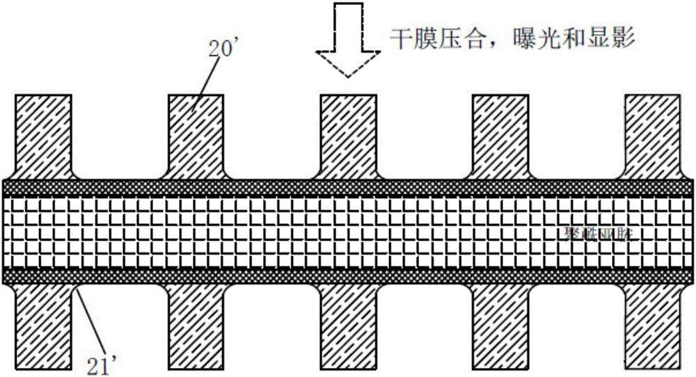
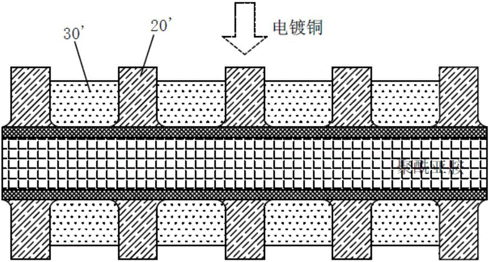
[0029] ginseng Figure 1a ~ Figure 1e Shown is the process flow chart of the manufacturing method of the thin circuit layer flexible circuit board in the prior art, including the following steps:

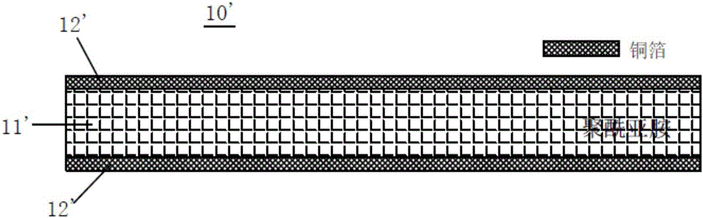
[0030] ginseng Figure 1a As shown, a substrate 10' is provided. The substrate 10' includes a substrate layer 11' and metal layers 12' loc...


PUM


Abstract

The invention discloses a manufacturing method of a flexible circuit board with a thin circuit layer having a square-shaped cross section. The manufacturing method comprises the steps that a substrate is provided, wherein the substrate comprises a base material layer and a metal layer located on at least one side of the base material layer; dry film pressing, exposure and development are conducted on the metal layer of the substrate; dry film residual foots formed after dry film development are cleared by utilizing plasma treatment, and a dry film having a square-shaped cross section is formed; metal is plated on the metal layer of the substrate to form an electroplated layer; the metal layer below a non-electroplated layer is etched to form the flexible circuit board, wherein the circuit layer on the flexible circuit board comprises the metal layer having the square-shaped cross section and the electroplated layer. The dry film residual foots are subjected to plasma treatment after dry film development, the dry film having the square-shaped cross section is achieved, further the circuit layer cross section of the product is square finally, the contact area and bonding power of the circuit layer and the base material layer are improved, and the product yield is finally improved.

Description

technical field [0001] The invention relates to the technical field of flexible circuit boards, in particular to a method for manufacturing a thin circuit layer with a square cross-sectional shape of a flexible circuit board. Background technique [0002] With the miniaturization of electronic products, the requirements for high-density wiring of flexible circuit boards are getting higher and higher, so thinner line width and line spacing have become the development trend of the market. The limit ability of the existing etching circuit process to make thin lines is about 25 / 25 microns in line width / line spacing, which is powerless to produce thinner line width and line spacing, so a new process semi-additive method was developed. The new process can be used to make ultra-fine lines with a line width / space below 25 / 25 microns. The substrate material of the semi-additive method for making double-sided panels is a middle layer of polyimide with a thickness of 25 microns, and t...

Claims


Application Information

Patent Timeline
IPC IPC(8): H05K3/10
CPCH05K3/108H05K2203/095
Inventor 刘清
Owner 苏州维信电子有限公司
Why Eureka
Try Eureka