MOSFET integrated with Schottky diode
A region and groove technology, applied in the direction of electrical components, electrical solid devices, circuits, etc., can solve the problems of high reverse bias leakage current, large chip area, poor device performance, etc., to increase the area and reduce the forward conduction Effect of Voltage, Small Chip Area
- Summary
- Abstract
- Description
- Claims
- Application Information
AI Technical Summary
Problems solved by technology
Method used
Image

Examples
no. 1 example
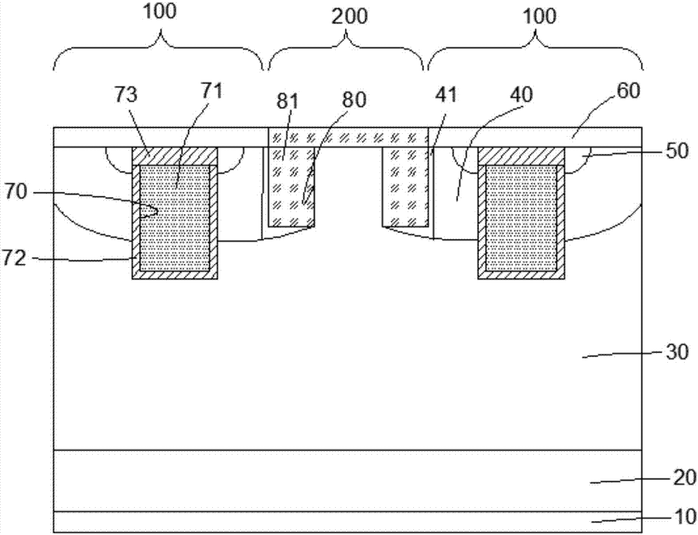
[0024] Such as figure 1 As shown, this embodiment integrates Schottky MOSFETs, including: a MOSFET region 100 and a Schottky region 200 between two MOSFET regions 100, and the MOSFET region 100 includes drain electrodes 10 stacked sequentially from bottom to top, The N-type heavily doped region 20, the N-type drift region 30, the P-type doped region 40, the N-type doped region 50, the source electrode 60, and the N-type doped region 50 and the P-type doped region 60 extending to the N-type The first trench 70 in the drift region 30, the first trench 70 is filled with conductive polysilicon 71, and the sidewall and bottom of the first trench 70 form a gate insulating layer 72, the conductive polysilicon 71 and the source electrode 60 are separated by an insulating medium 73, a Schottky region 200 is formed between two adjacent MOSFET regions 100, and the upper surface of the N-type drift region 30 of the Schottky region 200 is connected to the N-type drift region 30 of the MOSF...
no. 2 example
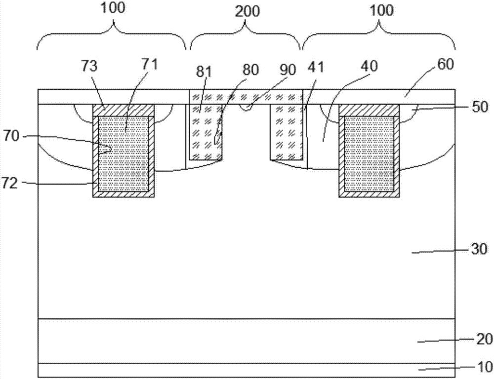
[0029] Such as figure 2 As shown, the technical solution of this embodiment is basically the same as that of the first embodiment. The impurity method can be doped by ion implantation. When the Schottky diode is in the reverse bias state, the P-type protection region 90 and the N-type drift region 30 form a PN depletion, which reduces the reverse leakage current and increases the reverse withstand voltage capability. .
no. 3 example
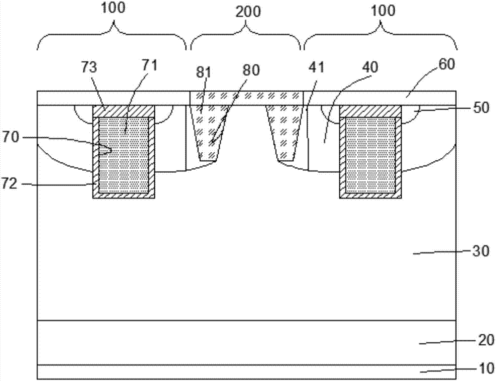
[0031] Such as image 3As shown, the technical solution of this embodiment is basically the same as that of the first embodiment, the difference is that the second groove 80 in this embodiment is an oblique groove, and the setting of the oblique groove can alleviate the Schottky diode in the MOSFET from being in the reverse direction. In the bias state, the electric field at the bottom and top corners of the trench gathers to increase the directional withstand voltage capability and reduce the reverse leakage current.
PUM
 Abstract
Description
Claims
Application Information
 - R&D
- Intellectual Property
- Life Sciences
- Materials
- Tech Scout
- Unparalleled Data Quality
- Higher Quality Content
- 60% Fewer Hallucinations
Browse by: Latest US Patents, China's latest patents, Technical Efficacy Thesaurus, Application Domain, Technology Topic, Popular Technical Reports.
© 2025 PatSnap. All rights reserved.Legal|Privacy policy|Modern Slavery Act Transparency Statement|Sitemap|About US| Contact US: help@patsnap.com