A kind of ceramic metallized film and preparation method thereof
A technology of ceramic metallization and ceramic metal, applied in metal material coating process, vacuum evaporation coating, coating and other directions, can solve the problems of large thickness of metallization layer, high cost, high sintering temperature, and reduce the loss of thermal expansion coefficient. The effect of matching, tensile strength improvement, and precise control of ceramic size
- Summary
- Abstract
- Description
- Claims
- Application Information
AI Technical Summary
Problems solved by technology
Method used
Image
Examples
Embodiment 1
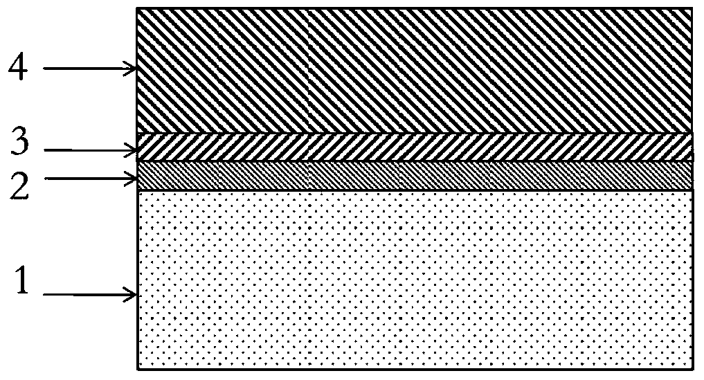
[0019] 1)Al 2 o 3 The substrate was cleaned with acetone and alcohol, and Ti / Al was prepared by magnetron co-sputtering 2 o 3 transition layer. Using metal Ti target and ceramic Al 2 o 3 target, vacuum cavity back vacuum is better than 2.0×10 -3 pa, Ti target power is 60W, Al 2 o 3 The target power is 100W, the working pressure is 1.5Pa, and the deposition time is 90 minutes. The transition layer has a thickness of 150 nm and a Ti content of 45 at%.
[0020] 2) on Ti / Al 2 o 3 The Ti layer is prepared by magnetron sputtering on the transition layer, using a metal Ti target, and the vacuum at the back of the vacuum chamber is better than 2.0×10 -3 pa, the Ti target power is 100W, the working pressure is 1.5Pa, and the deposition time is 30 minutes. The thickness of the Ti film is 100 nm.
[0021] 3) The Ni layer is prepared on the Ti layer by magnetron sputtering method, using a metal Ni target, and the vacuum at the back of the vacuum chamber is better than 2.0×10 ...
Embodiment 2
[0025] 1)Al 2 o 3 The substrate was cleaned with acetone and alcohol, and Ti / Al was prepared by magnetron co-sputtering 2 o 3 transition layer. Using metal Ti target and ceramic Al 2 o 3 target, vacuum cavity back vacuum is better than 2.0×10 -3 Pa, Ti target power is 80W, Al 2 o 3 The target power is 100W, the working pressure is 1.5Pa, and the deposition time is 80 minutes. The transition layer has a thickness of 130 nm and a Ti content of 75 at%.
[0026] 2) on Ti / Al 2 o 3 The Ti layer is prepared by magnetron sputtering on the transition layer, using a metal Ti target, and the vacuum at the back of the vacuum chamber is better than 2.0×10 -3 pa, the Ti target power is 100W, the working pressure is 1.5Pa, and the deposition time is 30 minutes. The thickness of the Ti film is 100 nm.
[0027] 3) The Ni / Mo layer was prepared on the Ti layer by magnetron sputtering, and the Ni / Mo alloy target was used, and the vacuum at the back of the vacuum chamber was better th...
Embodiment 3
[0031] 1) The SiC substrate was cleaned with acetone and alcohol, and the Nb / SiC transition layer was prepared by magnetron co-sputtering. Metal Nb target and ceramic SiC target are used, and the vacuum at the back of the vacuum chamber is better than 2.0×10 -3 pa, the Nb target power is 50W, the SiC target power is 100W, the working pressure is 1.5Pa, and the deposition time is 70 minutes. The transition layer has a thickness of 120 nm and a Nb content of 25 at%.
[0032] 2) On the Nb / SiC transition layer, the Nb layer is prepared by magnetron sputtering, using a metal Nb target, and the vacuum at the back of the vacuum chamber is better than 2.0×10 -3 pa, the Nb target power is 100W, the working pressure is 1.5Pa, and the deposition time is 24 minutes. The thickness of the Nb thin film is 80nm.
[0033] 3) On the Nb layer, the Ni / Mo layer was prepared by magnetron sputtering, and the Ni / Mo alloy target was used, and the vacuum at the back of the vacuum chamber was better ...
PUM
| Property | Measurement | Unit |
|---|---|---|
| thickness | aaaaa | aaaaa |
| thickness | aaaaa | aaaaa |
| thickness | aaaaa | aaaaa |
Abstract
Description
Claims
Application Information
