Microscopic imaging technique compounding surface plasma resonance and surface enhanced raman

A surface-enhanced Raman and plasma technology, applied in Raman scattering, measuring devices, instruments, etc., can solve the problems of inability to detect biologically, high production costs, lack of nanostructure enhanced local field strength, etc.

Active Publication Date: 2017-06-27
SICHUAN UNIV
View PDF6 Cites 11 Cited by
  • Summary
  • Abstract
  • Description
  • Claims
  • Application Information

AI Technical Summary

Problems solved by technology

However, its enhancement method only enhances the Raman signal through surface plasmon resonance, and lacks nanostructures to enhance the local field strength, resulting in a low enhancement rate and high-precision biological detection.
[0004] The above methods can achieve surface plasmon-enhanced Ra...

Method used


Image

  • Microscopic imaging technique compounding surface plasma resonance and surface enhanced raman
  • Microscopic imaging technique compounding surface plasma resonance and surface enhanced raman
  • Microscopic imaging technique compounding surface plasma resonance and surface enhanced raman

Examples


Embodiment Construction

[0024] All features disclosed in this specification, or steps in all methods or processes disclosed, may be combined in any manner, except for mutually exclusive features and / or steps.

[0025] Any feature disclosed in this specification, unless specifically stated, can be replaced by other alternative features that are equivalent or have similar purposes. That is, unless expressly stated otherwise, each feature is only one example of a series of equivalent or similar features.

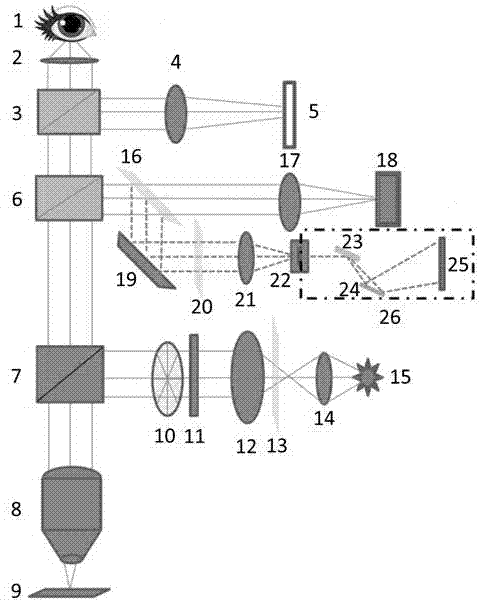
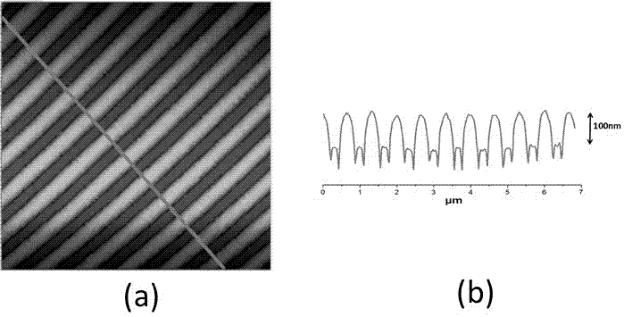
[0026] use figure 2 Composite biochip shown: a common grating structure is parametrically coupled to form a new grating, a nano-gap is formed between the old and new gratings, and there are two nano-gaps on the order of 10 nanometers in one period; the composite chip has a grating period of about 400 or 600 nanometers The slit array structure corresponds to the SPR excitation wavelength of 633 or 785 nm. For the microscopic illumination system, the parallel light is focused by the microscopic objec...


PUM


Abstract

The invention discloses a microscopic imaging technique compounding surface plasma resonance (SPR) and surface enhanced Raman scattering (SERS) and relates to the field of surface plasma elements and surface enhanced Raman scattering. The technical key point disclosed by the invention is as follows: an SPR-SERS comprehensive microscopic imaging system is assembled, and SPR and SERS are excited and detected by a nano slit array raster bi-model structure; an SPR system judges change of an exciting angle by measuring movement of an SPR peak position to determine change of the surface effective refractive index induced by a biomolecular reaction on the surface of a chip; the SERS system directly differentiates the biomolecules by measuring the Raman spectrum; efficient and high-sensitive detection of SPR and Raman is dependent on the nano slit array raster bi-model structure: the excitation wavelength efficiently excites SPR through the raster structure; SPR generates dipole vibration in nanogaps in a metal surface spreading process, and the surface electric field generated by SPR and the nano silt dipole jointly act to enhance the surface local electric field to acquire an enhanced Raman signal.

Description

technical field [0001] The invention relates to the field of surface plasmon elements and surface-enhanced Raman, a large-area periodic nano-slit array structure excites plasmon resonance and surface-enhanced Raman, and a microscopic imaging of composite surface plasmon resonance and surface-enhanced Raman technology. Background technique [0002] Surface Plasmon Resonance (SPR) is a quantum photoelectric phenomenon in which photons are incident on the surface of a noble metal, causing the electrons in the metal to oscillate with the electric field. SPR technology detects biomolecules by measuring the change of excitation coupling conditions caused by the change of surface effective refractive index after the interaction of biological substances on the metal interface, which is an indirect measurement; while Raman signal detection is a complete method. Measure directly. Raman scattering is the inelastic scattering of incident light by the sample to be measured. Its essence...

Claims


Application Information

Patent Timeline
IPC IPC(8): G01N21/65G01N21/552
CPCG01N21/554G01N21/658
Inventor 李文雪时元振庞霖
Owner SICHUAN UNIV
Why Eureka
Try Eureka