Packaging structure of a semiconductor chip

A packaging structure and semiconductor technology, applied in the field of microelectronics, can solve problems such as uneven heat dissipation of semiconductor chips, and achieve the effects of solving uneven heat dissipation, increasing area, and reducing thermal resistance

Active Publication Date: 2019-11-05
昆山工研院第三代半导体研究院有限公司
View PDF6 Cites 0 Cited by
  • Summary
  • Abstract
  • Description
  • Claims
  • Application Information

AI Technical Summary

Problems solved by technology

[0004] The purpose of the present invention is to provide a packaging structure for semiconductor chips, aiming at improving the problem of uneven heat dissipation of semiconductor chips

Method used


Image

  • Packaging structure of a semiconductor chip
  • Packaging structure of a semiconductor chip
  • Packaging structure of a semiconductor chip

Examples


no. 1 example

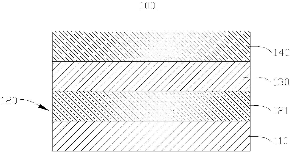
[0038] see figure 1 , The packaging structure 100 for semiconductor chips provided in this embodiment includes: a metal carrier layer 110 , a first thermal diffusion layer 120 , a thermally conductive adhesive layer 130 and a semiconductor chip 140 . The first thermal diffusion layer 120 is located on the metal carrier layer 110 , the thermally conductive adhesive layer 130 is located on the first thermal diffusion layer 120 , and the semiconductor chip 140 is located on the thermally conductive adhesive layer 130 . That is, both the first thermal diffusion layer 120 and the thermally conductive adhesive layer 130 are located between the metal carrier layer 110 and the semiconductor chip 140 .

[0039] In this embodiment, the first thermal diffusion layer 120 is a graphene layer 121, and the graphene layer 121 is made of graphene. Graphene is a flat film of carbon atoms that can be as thin as one carbon atom thick. The plane thermal conductivity of graphene is very good, and...

no. 2 example

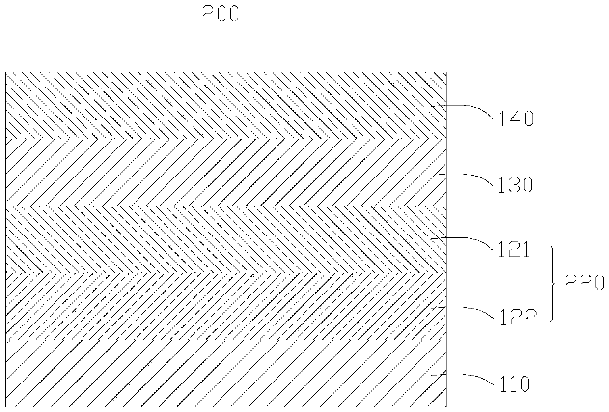
[0048] see figure 2 The semiconductor chip packaging structure 200 provided in this embodiment is substantially the same in structure as the semiconductor chip packaging structure 100 provided in the first embodiment. The difference between them is that, in this embodiment, the first thermal diffusion layer 220 includes a graphene layer 121 and a metal bonding layer 122 , and the metal bonding layer 122 is located between the graphene layer 121 and the metal carrier layer 110 . In this embodiment, the number of metal bonding layers of the first thermal diffusion layer 320 is equal to the number of graphene layers, and one layer of graphene layer 121 and one layer of metal bonding layer 122 are stacked to form a metal carrier layer 110. The first thermal diffusion layer 220 . Specifically, the metal bonding layer 122 may be made of copper, aluminum, copper molybdenum, copper tungsten, and the like. Copper, aluminum, copper molybdenum and copper tungsten not only have better ...

no. 3 example

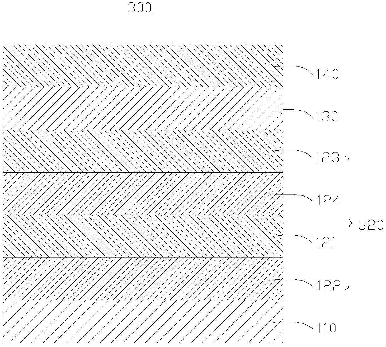
[0050] see image 3 The semiconductor chip packaging structure 300 provided in this embodiment is substantially the same in structure as the semiconductor chip packaging structure 200 provided in the second embodiment. The difference between the two is that, in this embodiment, the first thermal diffusion layer 320 includes a graphene layer 121 , a metal bonding layer 122 , a graphene layer 123 and a metal bonding layer 124 that are stacked on top of each other. The first thermal diffusion layer 320 is located between the thermally conductive adhesive layer 130 and the graphene layer 121 . Specifically, the graphene layer 123 is located on the metal bonding layer 124, and between the thermally conductive adhesive layer 130 and the metal bonding layer 124, and the metal bonding layer 124 is located on the graphene layer 121, and is positioned between the graphene layer 123 and graphite. Between the graphene layer 121, the graphene layer 121 is located on the metal bonding laye...


PUM


Abstract

The invention relates to the technical field of microelectronics, and provides a packaging structure of a semiconductor chip. The packaging structure comprises a metal carrier layer, a first diffusion layer, a heat conduction adhesive layer, and a semiconductor chip. The first diffusion layer is positioned on the metal carrier layer. The heat conduction adhesive layer is arranged on the diffusion layer. The semiconductor chip is arranged on the heat conduction adhesive layer. The first diffusion layer at least includes a graphene layer. The first diffusion layer at least includes the graphene layer and the thermal conduction of the graphene layer exhibits anisptropic properties. Therefore, heat exchange areas are increased, the problem of uneven heat radiation of the heat conduction adhesive layer caused by heat sources of the chip is solved, thermal resistance between the chip and the metal carrier layer is reduced, and the thermal conductance efficiency of the chip is improved.

Description

technical field [0001] The present invention relates to the technical field of microelectronics, in particular, to a package structure of a semiconductor chip. Background technique [0002] With the development of semiconductor technology, the volume of semiconductor chips is getting smaller and smaller, but the power is getting bigger and bigger. The demand for such high power density chips is showing a trend of rapid growth, especially in the field of microwave radio frequency. Common high power density chips, such as Gallium Nitride High Electron Mobility Transistors (GaN HEMTs) and Gallium Arsenide High Electron Mobility Transistors (GaAs HEMTs), can easily lead to chip or usage failure if effective thermal design and management are not carried out. The chip's system is not working properly due to overheating. [0003] High-power-density chips such as GaN HEMTs are prone to high temperatures during operation, especially hot spots with extremely high temperatures near th...

Claims


Application Information

Patent Timeline
Patent Type & Authority Patents(China)
IPC IPC(8): H01L23/373
CPCH01L23/3733H01L23/3735
Inventor 裴风丽
Owner 昆山工研院第三代半导体研究院有限公司
Why Eureka
Try Eureka