Silicon optical integration-based photon analog-to-digital conversion chip

An analog-to-digital conversion and chip technology, applied in optical analog/digital converters, optics, instruments, etc., can solve the problems of low precision, difficulty in improving or decreasing the performance of electronic analog-to-digital converters, etc., and achieve increased repetition rate, power Low power consumption and high stability

Active Publication Date: 2017-07-07
SHANGHAI JIAO TONG UNIV
View PDF4 Cites 12 Cited by
  • Summary
  • Abstract
  • Description
  • Claims
  • Application Information

AI Technical Summary

Problems solved by technology

[0003] The development of existing analog-to-digital converters is limited by the bottleneck of electronic devices, and the performance of a single electronic analog-to-digital converter (EADC) has been difficult to improve
The performance of the electronic analog-to-digital converter decreases continuously with the increase of the sampling frequency: when the sampling frequency increases from 2MHz to 4GHz, the resolution decreases by 1 bit for every doubling of the sampling frequency; the higher the sampling rate, the greater the jitter and the higher the accuracy Low

Method used


Image

  • Silicon optical integration-based photon analog-to-digital conversion chip
  • Silicon optical integration-based photon analog-to-digital conversion chip
  • Silicon optical integration-based photon analog-to-digital conversion chip

Examples


Embodiment Construction

[0028] The embodiments of the present invention will be described in detail below in conjunction with the accompanying drawings and Examples. This embodiment is implemented on the premise of the technical solution of the present invention, and detailed implementation methods and operating procedures are provided, but the protection scope of the present invention is not limited to Examples described below.

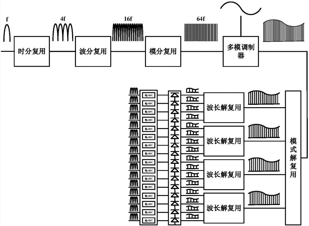
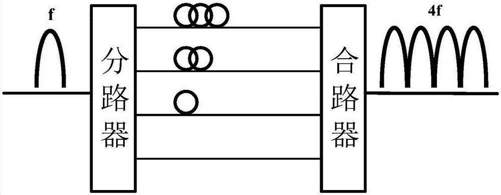
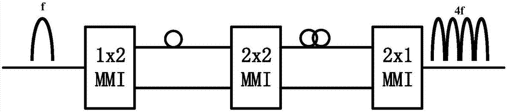
[0029] figure 1 It is a structural schematic diagram of an embodiment of the PADC system based on silicon-based optical integration of the present invention. It can be seen from the figure that the photonic analog-to-digital conversion chip based on silicon-based optoelectronic integration of the present invention has the following units from left to right: time division multiplexing unit, wavelength division multiplexing unit, mode division multiplexing unit, multimode modulator, mode decomposition A multiplexing unit, a wave division multiplexing unit, a photodetector an...


PUM


Abstract

The invention discloses a silicon optical integration-based photon analog-to-digital conversion chip, which comprises a time-division multiplexing unit, a wavelength-division multiplexing unit, a mode-division multiplexing unit, a multi-mode modulator, a mode demultiplexing unit, a wavelength demultiplexing unit and a photoelectric detection unit, wherein various components are monolithically integrated on the same silicon chip. The repetition frequency of an input light pulse of a light wave is further improved through different polarization modes and different waveguide modes, thereby more easily achieving optical analog-to-digital conversion with a high sampling rate.

Description

technical field [0001] The invention relates to technologies such as time division multiplexing (OTDM), wavelength division multiplexing (WDM), polarization multiplexing (PDM) and mode division multiplexing (MDM) in optical communication, and is a photonic analog digital system based on silicon optical integration. Signal conversion SoC. Background technique [0002] With the continuous expansion of scientific research fields, the bandwidth of analog signals that need to be processed in scientific research is getting higher and higher. During the transmission and processing of analog signals, noise is easily introduced, resulting in signal distortion. Digitizing the analog signal can bring many advantages, especially during the transmission and processing of the digital signal, no additional noise will be introduced, and the accuracy of the signal can be maintained. Between broadband analog signals and high-performance digital processing technology, high-performance analog...

Claims


Application Information

Patent Timeline
Patent Type & Authority Applications(China)
IPC IPC(8): G02F7/00
CPCG02F7/00
Inventor 周林杰景嘉钰王心怡陆梁军吴龟灵陈建平
Owner SHANGHAI JIAO TONG UNIV
Why Eureka
Try Eureka