Multi-epitaxial semiconductor device and manufacturing method thereof
A manufacturing method and semiconductor technology, applied in the fields of semiconductor/solid-state device manufacturing, semiconductor devices, electric solid-state devices, etc., can solve the problems of size reduction, cost increase, unfavorable cost savings, etc. The effect of competitiveness
- Summary
- Abstract
- Description
- Claims
- Application Information
AI Technical Summary
Problems solved by technology
Method used
Image

Examples
Embodiment 1
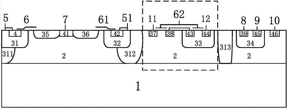
[0039] Figure 4 Shown is a schematic diagram of the structure of a multi-epitaxial semiconductor device of the present invention, its cellular structure includes a multi-epitaxial semiconductor device, its cellular structure includes a substrate 1, a first epitaxial layer 2, a second epitaxial layer 21, a first STI isolation 131, second STI isolation 132, third STI isolation 133, first P well 31, third P well 33, fourth P well 34, DMOS source P-type heavily doped region 310, third P-type heavily doped region Doped region 37, fourth P-type heavily doped region 38, fifth P-type heavily doped region 39, DMOS source N-type heavily doped region 4, DMOS drain N-type heavily doped region 41, second N-type heavily doped region Type heavily doped region 43, the third N type heavily doped region 44, the fourth N type heavily doped region 45, the fifth N type heavily doped region 46, the DMOS source electrode 5, the contact electrode of the first P well 31 51, DMOS gate electrode 6, PM...
Embodiment 2
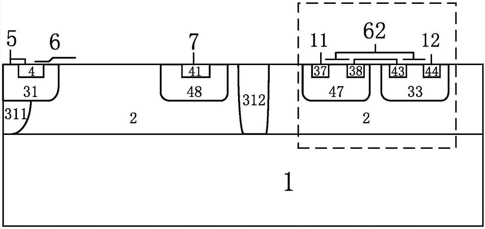
[0053] Such as image 3 As shown, this embodiment is basically the same as Embodiment 1, and the main difference is that the multi-epitaxial semiconductor device also includes a P Type doped region 314 , the upper surface of which is tangent to the upper surface of the second epitaxial layer 21 .
[0054] The manufacturing method of the above-mentioned multi-epitaxial semiconductor device is basically the same as the manufacturing method in Embodiment 1, the difference is that: P-type impurity ion implantation is performed after the growth of the second epitaxial layer 21 to form a P-type doped region 314, so that its upper surface and The upper surface of the second epitaxial layer 21 is tangential.
Embodiment 3
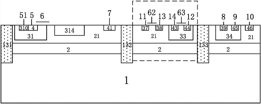
[0056] Such as Figure 5 As shown, this embodiment is basically the same as Embodiment 2, the main difference is that the P-type doped region 314 arranged between the first P well 31 and the N-type heavily doped region 41 of the DMOS drain, on which The surface is not tangent to the upper surface of the second epitaxial layer 21 .
[0057] The manufacturing method of the above-mentioned multi-epitaxial semiconductor device is basically the same as the manufacturing method in Embodiment 1, the difference is that: P-type impurity ion implantation is performed before the growth of the second epitaxial layer 21 to form a P-type doped region 314, so that the upper surface is not Tangent to the upper surface of the second epitaxial layer 21 .
PUM
 Abstract
Description
Claims
Application Information
 - R&D
- Intellectual Property
- Life Sciences
- Materials
- Tech Scout
- Unparalleled Data Quality
- Higher Quality Content
- 60% Fewer Hallucinations
Browse by: Latest US Patents, China's latest patents, Technical Efficacy Thesaurus, Application Domain, Technology Topic, Popular Technical Reports.
© 2025 PatSnap. All rights reserved.Legal|Privacy policy|Modern Slavery Act Transparency Statement|Sitemap|About US| Contact US: help@patsnap.com