Fabrication method of flash memory unit

A flash memory unit and control gate technology, which is applied in the fields of electrical components, semiconductor/solid-state device manufacturing, semiconductor devices, etc., can solve the problems that the 0.13μm process is no longer applicable, and achieve the effects of saving area, reducing resistance and high quality

Active Publication Date: 2017-07-25
INTEGRATED SILICON SOLUTION SHANGHAI
View PDF5 Cites 2 Cited by
  • Summary
  • Abstract
  • Description
  • Claims
  • Application Information

AI Technical Summary

Problems solved by technology

[0005] However, as the size of embedded 2T pMOS flash nodes becomes smaller and smaller, the existing 0.13μm process is no longer applicable

Method used


Image

  • Fabrication method of flash memory unit
  • Fabrication method of flash memory unit
  • Fabrication method of flash memory unit

Examples


Embodiment Construction

[0028] In the following description, many technical details are proposed in order to enable readers to better understand the application. However, those skilled in the art can understand that without these technical details and various changes and modifications based on the following implementation modes, the technical solution claimed in each claim of the present application can be realized.

[0029] In order to make the purpose, technical solution and advantages of the present invention clearer, the following will further describe the implementation of the present invention in detail in conjunction with the accompanying drawings.

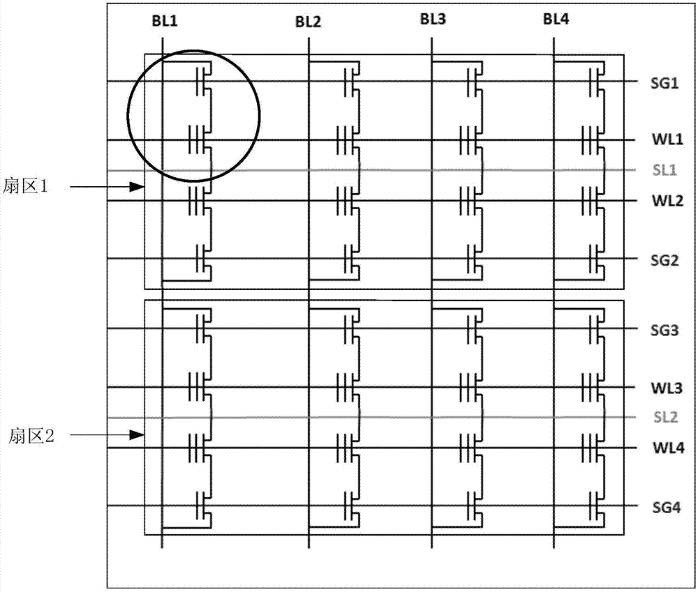
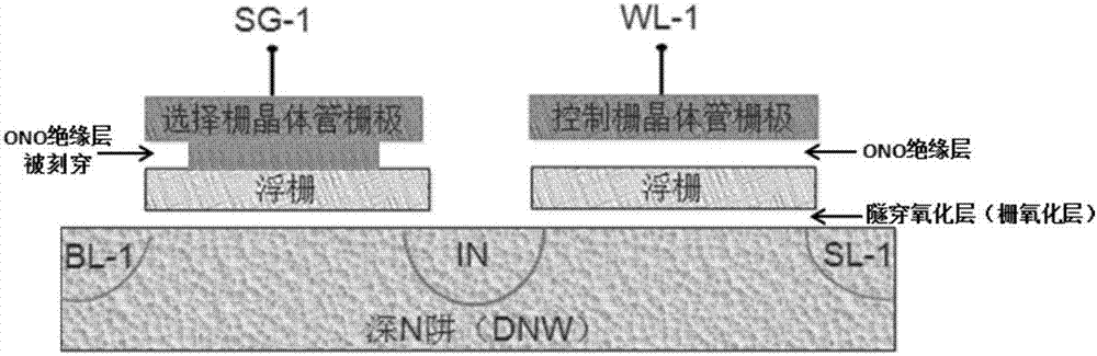
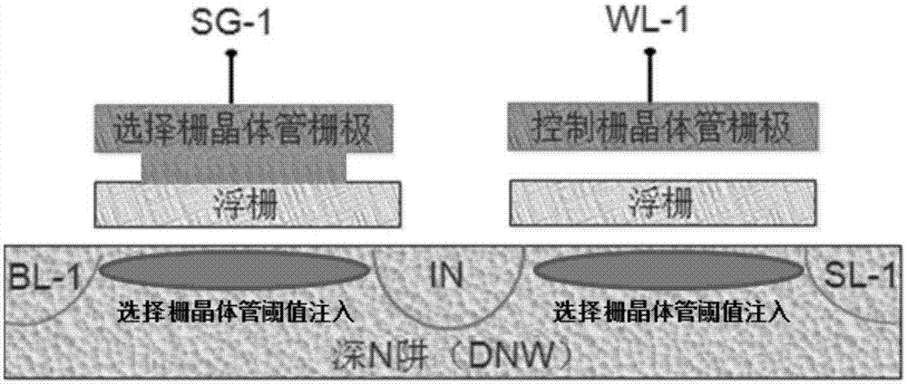
[0030] The embedded pMOS flash memory array involved in this application adopts a 2T pMOS unit structure. Such as figure 2 As shown, the flash memory cell is formed by a select gate PMOS transistor (SG-1 controls its gate potential) and a control gate PMOS transistor (WL-1 controls its gate potential) in series. Usually in a 0.13μm 2T pMOS cell...


PUM


Abstract

The invention relates to a fabrication method of a semiconductor device, and discloses a fabrication method of a flash memory unit. According to the fabrication method of the flash memory unit, P-type impurity injected to a logic grate of a select gate P-channel metal oxide semiconductor (PMOS) transistor region is diffused to an N-type floating gate poly-silicon layer by a subsequent high-temperature process after the logic gate of the select gate PMOS transistor region and a logic gate of a control gate PMOS transistor region are separated, so that an N-type floating gate is changed to a P-type floating gate, a select gate PMOS transistor with a surface channel having a relatively threshold value can be successfully fabricated on the flash memory unit with a size being 55 nanometers, and mass production is achieved. Moreover, by the process of growing the logic gates and the process of separating the logic gates, the floating gate doping of the control gate PMOS transistor cannot be affected as well as the surface channel, having the relatively threshold value, of the select gate PMOS transistor is formed.

Description

technical field [0001] The invention relates to a preparation method of a semiconductor device, in particular to a preparation method of a flash memory unit. Background technique [0002] Embedded 2T_pFlash Memory (Embedded 2T_pFlash Memory) is usually integrated into system-level chips in the form of IP (Intellectual Property, intellectual property rights), such as mobile phone SIM card (Subscriber Identity Module card, referred to as "SIM card") chips, smart bank card chips, MCU (Microprogrammed Control Unit, microprogram controller) chip and so on. Because of this feature, it is called "embedded" to distinguish it from products formed by Stand-alone Flash Memory. [0003] A single device unit is composed of two P-type metal oxide semiconductor (Metal Oxide Semiconductor Field, "MOS" for short) transistors (select gate transistor and control gate transistor) connected in series, so it is called 2T_pFlash. PMOS transistors are the basic components of modern VLSI. PMOS ha...

Claims


Application Information

Patent Timeline
IPC IPC(8): H01L27/11524H01L27/11529H01L27/11531
CPCH10B41/42H10B41/41H10B41/35H10B41/30H01L29/66825H01L29/7841H01L29/42328H01L21/046H10B41/47H10B41/48H10B41/60
Inventor 沈安星林志光
Owner INTEGRATED SILICON SOLUTION SHANGHAI
Why Eureka
Try Eureka