Optical material for full lamination process and preparation method and application of optical material
An optical material, full lamination technology, applied in the field of full lamination, can solve the problems of complex process, inability to use, high cost of optical glue, and achieve the effect of simple processing process, high yield and good display performance
- Summary
- Abstract
- Description
- Claims
- Application Information
AI Technical Summary
Problems solved by technology
Method used
Image
Examples
preparation example Construction
[0044] A method for preparing an optical material used in a full bonding process includes the following steps:
[0045] S1: Provide an optical layer, and apply liquid optical glue on both sides of the optical layer to form a first optical glue film layer and a second optical glue film layer;
[0046] S2: sticking protective films on the outer surfaces of the first optical adhesive film layer and the second optical adhesive film layer respectively;
[0047] S3: Cut into multiple optical materials of predetermined size specifications.
[0048] Before step S1, it also includes preprocessing the optical layer. The preprocessing includes plasma cleaning the optical layer. The method of plasma cleaning belongs to the prior art and will not be repeated here.
[0049] In step S1, the liquid optical glue is coated, and the liquid optical glue is cured after the liquid optical glue spreads evenly. The curing treatment includes adopting physical and / or chemical methods to cause the liquid optica...
Embodiment 1
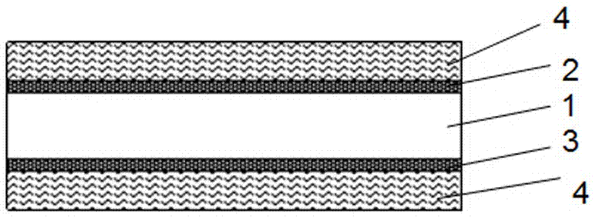
[0066] Refer to figure 1 , An optical material used in a full bonding process, comprising an optical layer having a first surface and a second surface opposite to the first surface, and the first surface of the optical layer is provided with a first optical Adhesive film layer, the second surface of the optical layer is provided with a second optical adhesive film layer, and the outer surfaces of the first optical adhesive film layer and the second optical adhesive film layer are respectively bonded with protective films.
[0067] The thickness of the optical layer is 0.1mm, the optical transmittance>90%, and the refractive index: 1.40; the optical layer is made of polycarbonate (PC), polystyrene (PS), polyethylene terephthalate Ester (PET), polymethyl methacrylate (PMMA), polypropylene (PP), polyethylene (PE), cellulose triacetate (TAC), polyvinyl chloride (PVC), polyacrylate (PA), poly Made of one or more of vinyl alcohol (PVA).
[0068] The thickness of the protective film is ...
Embodiment 2
[0071] Refer to figure 1 , An optical material used in a full bonding process, comprising an optical layer having a first surface and a second surface opposite to the first surface, and the first surface of the optical layer is provided with a first optical Adhesive film layer, the second surface of the optical layer is provided with a second optical adhesive film layer, and the outer surfaces of the first optical adhesive film layer and the second optical adhesive film layer are respectively bonded with protective films.
[0072] The thickness of the optical layer is 5.0 mm, the optical transmittance is >90%, and the refractive index is 1.55. The optical layer is made of polycarbonate (PC), polystyrene (PS), polyethylene terephthalate (PET), polymethyl methacrylate (PMMA), polypropylene (PP), polyethylene (PE), cellulose triacetate (TAC), polyvinyl chloride (PVC), polyacrylate (PA), polyvinyl alcohol (PVA) one or more of them.
[0073] The thickness of the protective film is 0.0...
PUM
| Property | Measurement | Unit |
|---|---|---|
| thickness | aaaaa | aaaaa |
| thickness | aaaaa | aaaaa |
| thickness | aaaaa | aaaaa |
Abstract
Description
Claims
Application Information
 - R&D
- Intellectual Property
- Life Sciences
- Materials
- Tech Scout
- Unparalleled Data Quality
- Higher Quality Content
- 60% Fewer Hallucinations
Browse by: Latest US Patents, China's latest patents, Technical Efficacy Thesaurus, Application Domain, Technology Topic, Popular Technical Reports.
© 2025 PatSnap. All rights reserved.Legal|Privacy policy|Modern Slavery Act Transparency Statement|Sitemap|About US| Contact US: help@patsnap.com

