Method for preparing polycrystalline SiC film through sapphire substrate

A sapphire substrate and thin film technology, which is applied in the growth of polycrystalline materials, chemical instruments and methods, crystal growth, etc., can solve the problems of poor SiC adhesion, large lattice mismatch, difficult nucleation and growth, etc., and achieve high working temperature , changing binding force and easy nucleation

Active Publication Date: 2017-08-18
NANJING UNIV OF AERONAUTICS & ASTRONAUTICS
View PDF3 Cites 2 Cited by
  • Summary
  • Abstract
  • Description
  • Claims
  • Application Information

AI Technical Summary

Problems solved by technology

[0004] But from the perspective of basic parameters, the lattice mismatch between the sapphire substrate (1) and the SiC thin film is ve

Method used


Image

  • Method for preparing polycrystalline SiC film through sapphire substrate
  • Method for preparing polycrystalline SiC film through sapphire substrate
  • Method for preparing polycrystalline SiC film through sapphire substrate

Examples


Embodiment Construction

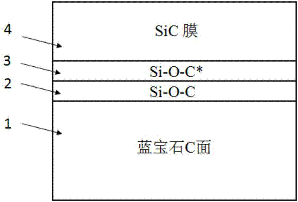
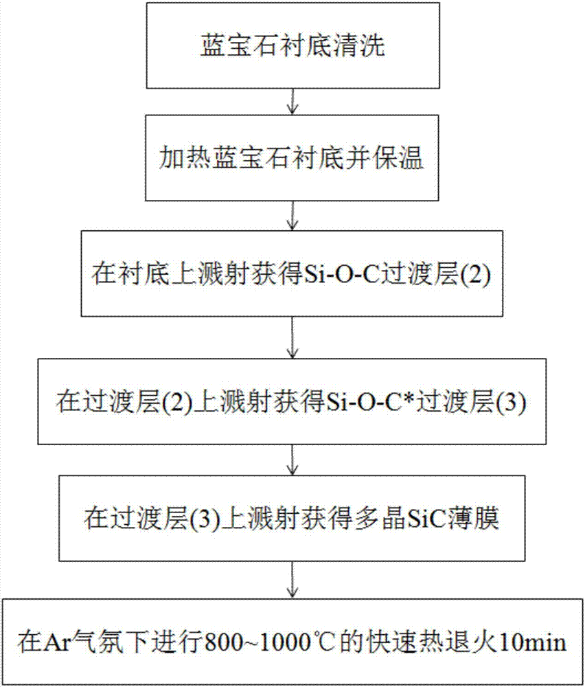
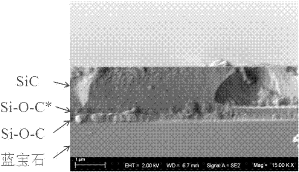
[0019] In order to enable those skilled in the art to better understand the technical solutions of the present invention, the present invention will be further described in detail below in conjunction with the accompanying drawings and specific embodiments. Hereinafter, embodiments of the present invention will be described in detail, examples of which are shown in the accompanying drawings, wherein the same or similar reference numerals denote the same or similar elements or elements having the same or similar functions throughout. The embodiments described below by referring to the figures are exemplary only for explaining the present invention and should not be construed as limiting the present invention. Those skilled in the art will understand that unless otherwise stated, the singular forms "a", "an", "said" and "the" used herein may also include plural forms. It should be further understood that the word "comprising" used in the description of the present invention refe...


PUM


Abstract

The embodiment of the invention discloses a method for preparing a polycrystalline SiC film through a sapphire substrate and relates to the technical field of semiconductor film materials. The method comprises the steps of putting the cleaned sapphire substrate (1) and an SiC target material into a vacuum reaction cavity, pumping the vacuum reaction cavity into a high vacuum state, and heating the sapphire substrate (1); introducing argon and oxygen into the vacuum reaction cavity and maintaining air pressure; executing a magnetron sputtering process to obtain a transition layer (1) and a transition layer (3), wherein the sputtering process comprises pre-sputtering and formal sputtering; closing an oxygen channel, only introducing argon and maintaining the air pressure; executing the magnetron sputtering process again to obtain an SiC film (4); cooling the vacuum reaction cavity to a room temperature and then taking out a sample; and putting the taken sample into a quick annealing oven for thermal annealing. The method is suitable for preparation of the polycrystalline SiC film on the sapphire substrate.

Description

technical field [0001] The invention relates to the technical field of semiconductor thin film materials, in particular to a method for preparing a polycrystalline SiC thin film through a sapphire substrate. Background technique [0002] Si is the representative of the first generation of narrow-bandgap semiconductor materials, and its usage occupies an absolute advantage in all semiconductor materials. Almost all power and power electronic devices are manufactured using Si materials, but Si materials are not completely ideal. For example, the temperature sensor made of Si material has an effective temperature measurement range of only 0-150°C, which cannot be adapted to the measurement in some high-temperature environments. Therefore, in recent years, the research on the third-generation wide bandgap semiconductor material, that is, SiC material, has gradually begun. SiC materials have superior electrical properties, and are especially suitable for making high-voltage, hig...

Claims


Application Information

Patent Timeline
IPC IPC(8): C30B28/12C30B29/36C30B33/02C23C14/35C23C14/58C23C14/06
CPCC23C14/0635C23C14/3492C23C14/35C23C14/5806C30B28/12C30B29/36C30B33/02
Inventor 杨颖姚靖懿王一平郑炳金王建业
Owner NANJING UNIV OF AERONAUTICS & ASTRONAUTICS
Why Eureka
Try Eureka