
A Surface-Enhanced Raman Substrate Fabrication Method Based on Electron Dynamic Control
A technology of surface-enhanced Raman and electronic dynamic regulation, which is applied in the fields of nanotechnology, Raman scattering, and material excitation analysis for materials and surface science. It can solve the problems of easy oxidation by air, uneven size of silver nanoparticles, and limited Wide application and other issues to achieve the effect of improving the enhancement factor, regulating the electron density, and good chemical stability
- Summary
- Abstract
- Description
- Claims
- Application Information
AI Technical Summary
Problems solved by technology
Method used
Image

Examples
Embodiment 1
[0034] A method for manufacturing a surface-enhanced Raman (SERS) substrate based on electronic dynamic regulation, the steps of which are as follows:
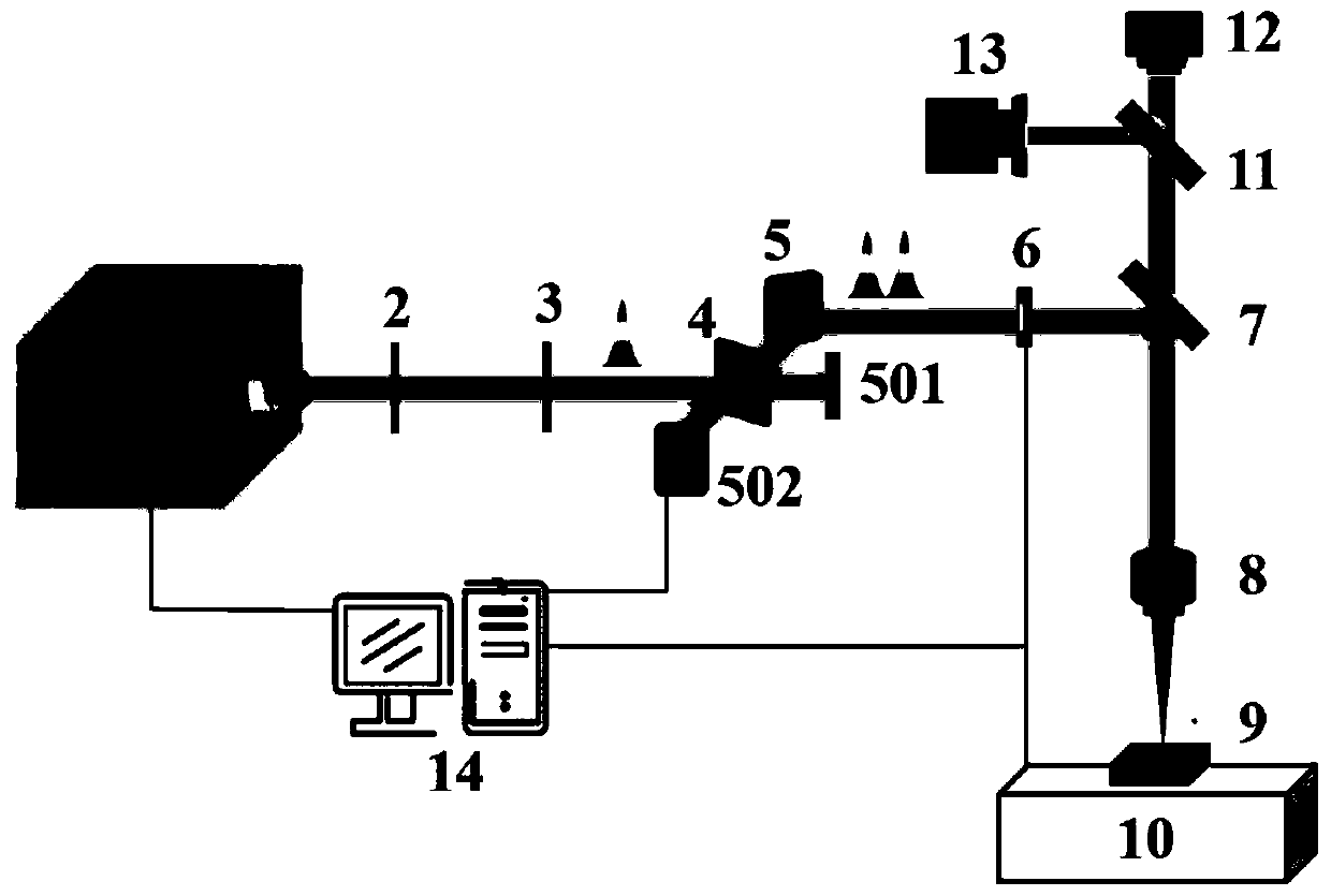
[0035] (1) build as figure 1 The femtosecond laser processing system shown;
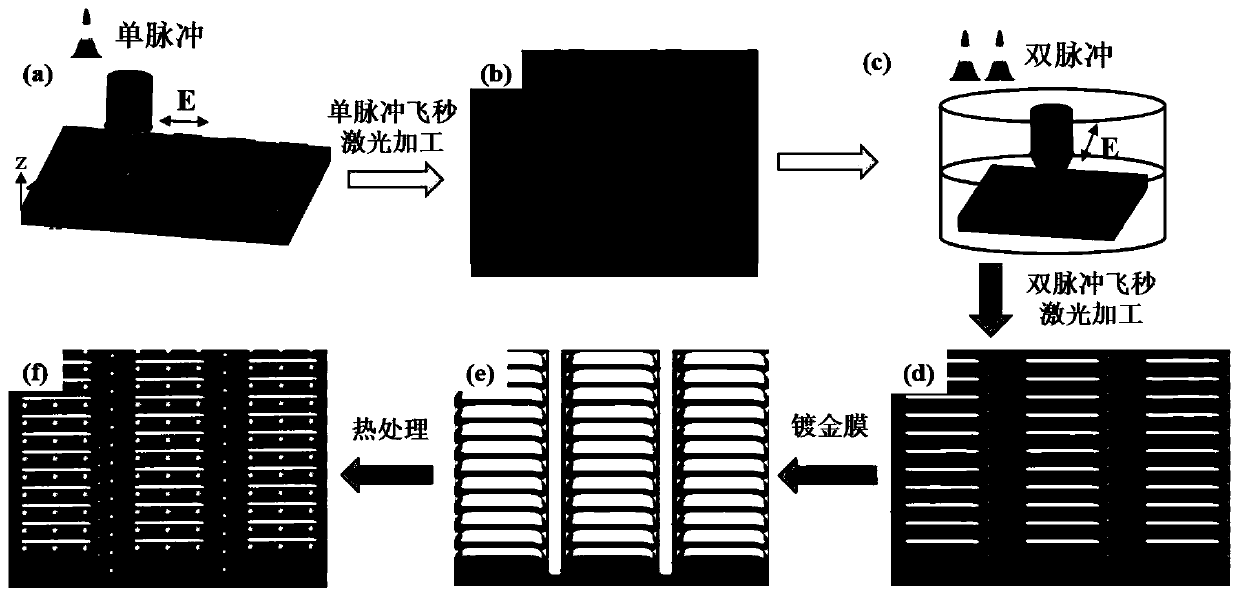
[0036] (2) if figure 2 As shown in (a), in air, a single-pulse femtosecond laser was used to fabricate such as figure 2 (b) The large-area, consistent surface corrugation structure shown;
[0037] (3) if figure 2 As shown in (c), in an aqueous solution, a double-pulse femtosecond laser is used to fabricate a substrate with a corrugated surface such as figure 2 (d) The large-area, consistent nanorod array structure shown;
[0038] (4) if figure 2 As shown in (e), the nanorod array substrate prepared by the femtosecond laser is coated with a nanometer-thick metal film by using the electron beam evaporation coating method; in this embodiment, a gold film is coated, and the thickness of the gold film is 15nm. However, those skilled in the art...
PUM
| Property | Measurement | Unit |
|---|---|---|
| thickness | aaaaa | aaaaa |
| thickness | aaaaa | aaaaa |
Abstract
Description
Claims
Application Information