Supercharge Your Innovation With Domain-Expert AI Agents!

Method and device for permanently repairing defects of absent material of a photolithographic mask

A photolithography mask, permanent technology, applied in metal material coating process, originals for photomechanical processing, optics, etc., to increase long-term stability

Pending Publication Date: 2017-09-05
CARL ZEISS SMT GMBH
View PDF6 Cites 2 Cited by
  • Summary
  • Abstract
  • Description
  • Claims
  • Application Information

AI Technical Summary

Problems solved by technology

[0010] However, applying a full-area protective layer on the repaired mask to cover one or more repair locations is a time and cost intensive additional process step
Again, depositing this additional layer carries the risk that a less than perfectly uniform layer will create new defects on the repaired photomask

Method used


Image

  • Method and device for permanently repairing defects of absent material of a photolithographic mask
  • Method and device for permanently repairing defects of absent material of a photolithographic mask
  • Method and device for permanently repairing defects of absent material of a photolithographic mask

Examples


Embodiment Construction

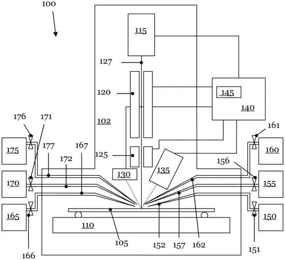
[0059] In the following, based on the example of a modified scanning electron microscope, a presently preferred embodiment of the device according to the invention for permanently repairing defects of material defects of photolithographic masks is explained in more detail. However, the device according to the invention is not limited to the examples described below. As the person skilled in the art will recognize without difficulty, instead of the scanning electron microscope in question, any scanning particle microscope using, for example, a focused ion beam and / or a focused photon beam as energy source may be employed. Furthermore, methods according to the present invention are not limited to the use of masks discussed through the following examples. Rather, the method can be used to repair any desired photolithographic mask. Furthermore, the application of the method according to the invention is not limited to application to photomasks. Conversely, the method can be used...


PUM

PropertyMeasurementUnit
diameteraaaaaaaaaa
thicknessaaaaaaaaaa

Abstract

The present application relates to a method for permanently repairing defects (260, 270, 280) of absent material of a photolithographic mask (105, 210, 220), comprising the following steps: (a) providing at least one carbon-containing precursor gas and at least one oxidizing agent at a location to be repaired of the photolithographic mask (105, 210, 220); (b) initiating a reaction of the at least one carbon-containing precursor gas with the aid of at least one energy source (127) at the location of absent material in order to deposit a material at the location of absent material, wherein the deposited material (460, 670, 880) comprises at least one reaction product of the reacted at least one carbon-containing precursor gas; and (c) controlling a gas volumetric flow rate of the at least one oxidizing agent in order to minimize a carbon proportion of the deposited material (460, 670, 880).

Description

technical field [0001] The present invention relates to a method and a device for permanently repairing defects of material defects of photolithography masks. Background technique [0002] In microelectronics, as a result of ever-increasing integration densities, photolithographic masks have to image ever smaller structural elements in the photoresist layer of the wafer. To meet these requirements, exposure wavelengths are shifting to shorter wavelengths. Currently, argon fluoride (ArF) excimer lasers are mainly used for exposure purposes, and these lasers emit at a wavelength of 193nm. Intensive work is continuing on light sources emitting in the extreme ultraviolet (EUV) wavelength range (10nm to 15nm) and corresponding EUV masks. In order to increase the resolving power of the wafer exposure process, many types of conventional binary photolithography masks have been developed simultaneously, examples of which are phase masks or phase shift masks and masks for multiple e...

Claims


Application Information

Patent Timeline
Patent Type & Authority Applications(China)
IPC IPC(8): G03F1/72
CPCG03F1/72C23C16/047C23C16/402C23C16/405C23C16/56H01J2237/31744H01J37/3178H01J2237/006H01J2237/30466H01L21/02205H01L21/02263H01L21/0274H01L21/485G03F1/74C23C14/28C23C14/30C23C16/18C23C16/16C23C16/483C23C16/486H01J37/30C23C14/048C23C14/083C23C14/085C23C14/10C23C14/221C23C14/548C23C14/5873G03F1/26
Inventor J.奥斯特K.科尔尼洛夫T.布雷特H.施耐德T.霍夫曼
Owner CARL ZEISS SMT GMBH
Features
  • R&D
  • Intellectual Property
  • Life Sciences
  • Materials
  • Tech Scout
  • Unparalleled Data Quality
  • Higher Quality Content
  • 60% Fewer Hallucinations
Learn More