Method of manufacturing semiconductor device and substrate processing apparatus

a technology of substrate processing and semiconductor devices, which is applied in the direction of coatings, chemical vapor deposition coatings, metallic material coating processes, etc., can solve the problems of poor step coverage, low throughput, and inability to achieve the desired film forming rate, so as to improve the coverage characteristics and the loading effect.

Inactive Publication Date: 2010-04-08
KOKUSA ELECTRIC CO LTD
View PDF4 Cites 180 Cited by
  • Summary
  • Abstract
  • Description
  • Claims
  • Application Information

AI Technical Summary

Benefits of technology

[0011]An object of the present invention is to provide a method of manufacturing a semiconductor device and a substrate processing apparatus that can be used to form an oxide film with improved coverage characteristics and loading effect without having to increase the supply amount or time of an oxidant.

Problems solved by technology

However, in a method of forming a metal oxide film at a low temperature by using an ALD method, for example, if a HfO2 film is formed in a state where O3 (oxidant) is not sufficiently activated, a desired film forming rate cannot be obtained, and other problems are caused: for example, the thickness of a HfO2 film is reduced at the center part of a pattern wafer having a trench structure to result in poor step coverage, or the coverage characteristics of HfO2 films are deteriorated according to the number of pattern wafers charged as a batch, or the thickness of a HfO2 film is varied according to the density of a pattern (this phenomenon is called “loading effect”).
If the supply amount or time of ozone (oxidant) is increased so as to increase the film forming rate or improve the step coverage or loading effect, although the step coverage or the loading effect can be improved owing to the increased film forming rate, since the film forming time is increased, throughput is decreased or raw material consumption is increased, and thus cost of ownership (COO: manufacturing costs per wafer) is increased.

Method used


Image

  • Method of manufacturing semiconductor device and substrate processing apparatus
  • Method of manufacturing semiconductor device and substrate processing apparatus
  • Method of manufacturing semiconductor device and substrate processing apparatus

Examples


embodiment 1

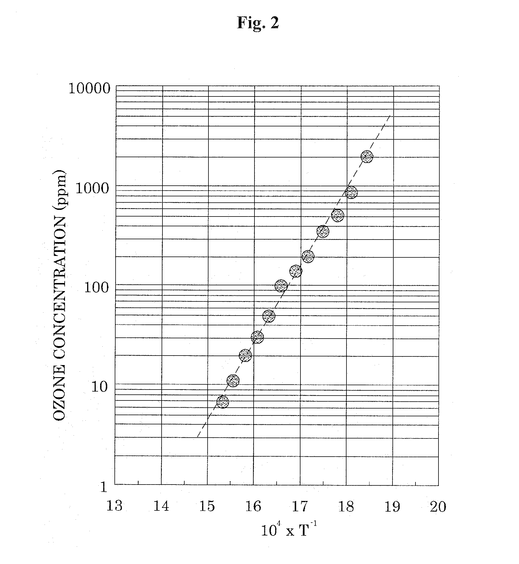
[0040]As shown in FIG. 2, the concentration of O3 in gas decreases as temperature increases.

[0041]For example, O3 is heated from the state of O3 / O2 17000 ppm, the concentration of O3 becomes about 350 ppm at 300° C. and changes to about 4 ppm at 400° C. That is, the concentration of O3 decreases to about 1 / 70 to 1 / 80 the initial value when the temperature increases by 100° C. from 300° C. to 400° C.

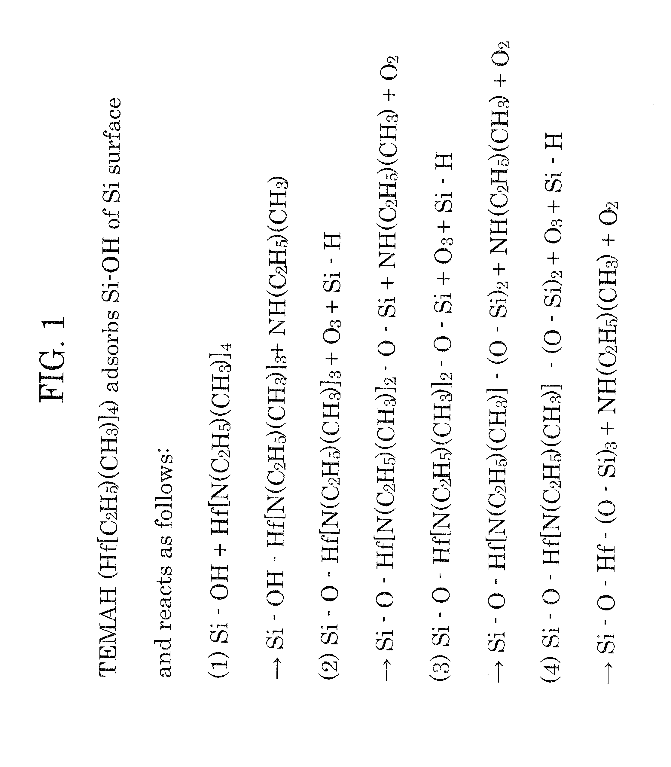
[0042]As shown in Formula 1, when the concentration of O3 decreases, 1 mole of O* generates as a result of decomposition of 1 mole of O3. That is, the amount of O* can be increased by about 70 to 80 times by increasing the temperature from 300° C. to 400° C. However, the concentration of generated O* decreases due to reverse reaction with O2 as shown by the reverse direction in Formula 1 or reaction with O3 as shown by Formula 2. To prevent this reaction, it is necessary to generate O* in the vicinity of a Si substrate. For this, according to a preferred embodiment of the present inventio...

embodiment 2

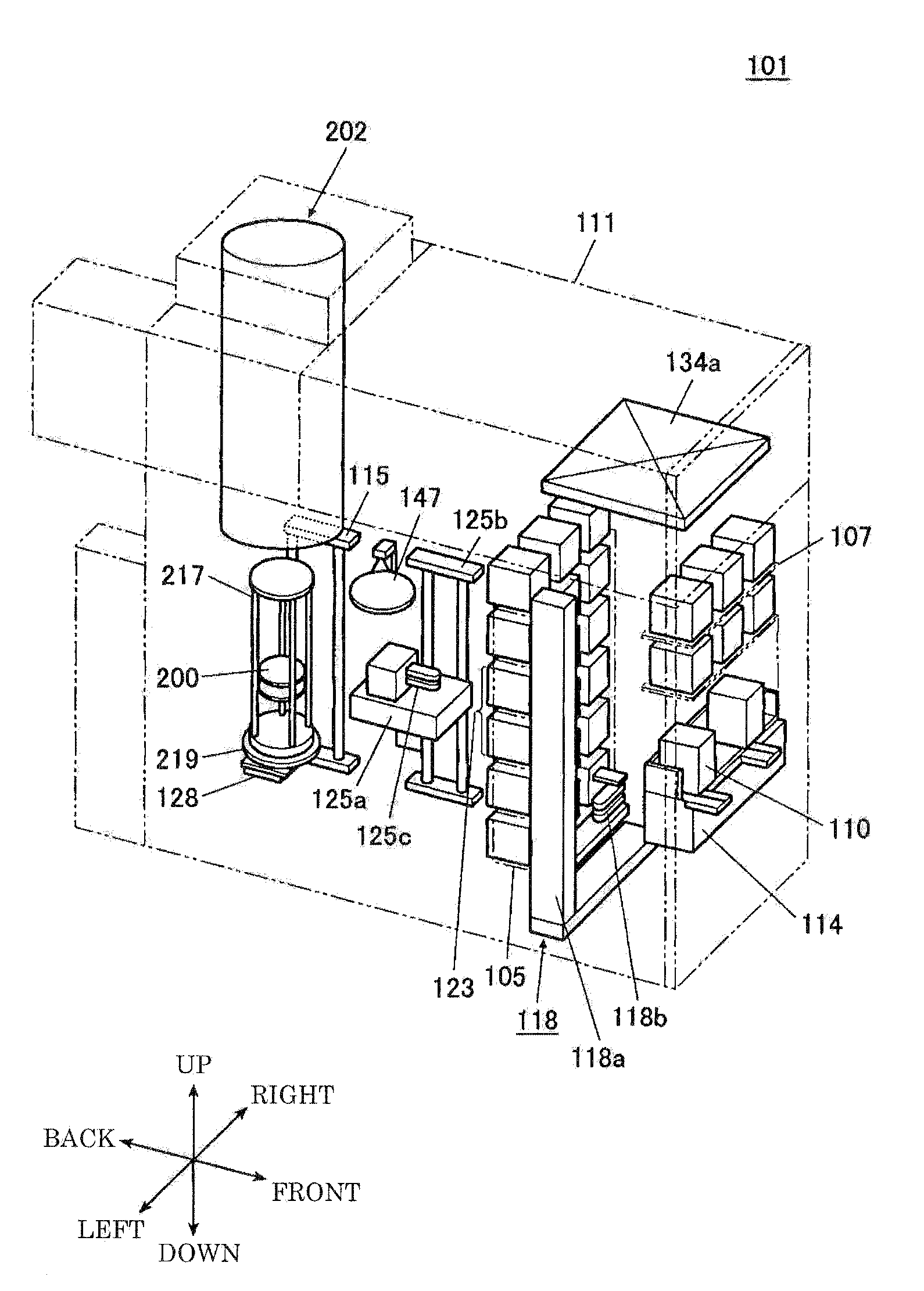
[0111]According to another embodiment of the present invention, an apparatus and method for manufacturing a semiconductor device will now be described in detail. A substrate processing apparatus 101 of Embodiment 2 is characteristically different, in that a mechanism configured to ultraviolet (UV) light is installed at a nozzle 233b instead of installing a heater 300 (heater wire) inside the nozzle 233b so as to heat a second reaction material such as O3 functioning as an oxidant.

[0112]At the nozzle 233b, a light source is installed as an UV generating mechanism so as to excite gas flowing through the nozzle 233b. The light source may emit light having any wavelength within the UV region. For example, the light source may be a vacuum ultraviolet (VUV) lamp that emits VUV light having a wavelength such as 146 nm, 172 nm, and 183 nm; a UV lamp that emits UV light having a main wavelength such as 222 nm, 308 nm, 248 nm, and 258 nm; or a mercury lamp.

[0113]As shown in FIG. 11, according...

embodiment 3

[0116]According to another embodiment using a mercury lamp or VUV lamp, a VUV lamp 510 can be installed in a nozzle 233b as shown in FIG. 12 and FIG. 13. Excimer is excited by silent discharge [dielectric barrier discharge].

[0117]The VUV lamp 510 includes a dielectric tube 520 made of a dielectric material such as quartz and having a hollow cylinder shape (dual structure), an outer electrode 530 installed outside the dielectric tube 520 and made of a metal having a net-like shape, and an inner electrode 531 installed inside the dielectric tube 520 and made of a metal. Discharge gas is filled in an inside area 550 of the dielectric tube 520 which is sealed. For example, Xe2 gas is enclosed. In addition, a high-frequency power source 540 is connected to the outer electrode 530 and the inner electrode 531 so that dielectric barrier discharge can occur at many places in the shape of a narrow wire between two dielectrics (quartz gap) by applying high-frequency power across the two electr...


PUM

PropertyMeasurementUnit
temperatureaaaaaaaaaa
thicknessaaaaaaaaaa
thicknessaaaaaaaaaa

Abstract

The coverage characteristics or loading effect of an oxide film can be improved without having to increase the supply amount or time of an oxidant. There is provided method of manufacturing a semiconductor device. The method comprises loading at least one substrate to a processing chamber; forming an oxide film on the substrate by alternately supplying a first reaction material and a second reaction material containing oxygen atoms to the processing chamber while heating the substrate; and unloading the substrate from the processing chamber, wherein the forming of the oxide film is performed by keeping the substrate at a temperature equal to or lower than a self-decomposition temperature of the first reaction material and irradiating ultraviolet light to the second reaction material.

Description

CROSS-REFERENCE TO RELATED PATENT APPLICATION[0001]This U.S. non-provisional patent application claims priority under 35 U.S.C. §119 of Japanese Patent Application Nos. 2008-260665, filed on Oct. 7, 2008, and 2009-179630, filed on Jul. 31, 2009, in the Japanese Patent Office, the entire contents of which are hereby incorporated by reference.BACKGROUND OF THE INVENTION[0002]1. Field of the Invention[0003]The present invention relates to a method of manufacturing a semiconductor device and a substrate processing apparatus, more particularly, to an effective technique for forming a metal oxide film on a process-target substrate.[0004]2. Description of the Prior Art[0005]Recently, as the integration level of semiconductor devices is highly increased, it is necessary to form a much thinner insulating film during a device forming process. However, since a tunnel current flows if the thickness of the insulating film is small, it is desired that the thickness of the insulating film is effec...

Claims


Application Information

Patent Timeline
Patent Type & Authority Applications(United States)
IPC IPC(8): H01L21/316C23C16/46C23C16/513
CPCC23C16/405C23C16/483H01L21/02164H01L21/02181H01L21/02189H01L21/31645H01L21/0228H01L21/3141H01L21/31608H01L21/31641H01L21/02277H01L21/31H01L21/265
Inventor MIYA, HIRONOBUTOYODA, KAZUYUKISAKAI, MASANORIMIZUNO, NORIKAZUKATO, TSUTOMUTAKEBAYASHI, YUJIONO, KENJIMORIKAWA, ATSUSHIOKADA, SATOSHI
Owner KOKUSA ELECTRIC CO LTD
Why Eureka
Try Eureka