

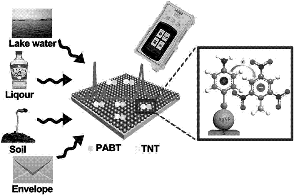
Silicon-based SERS chip, preparation method of silicon-based SERS chip and TNT detection method
A chip, silicon-based technology, applied in the detection of TNT, silicon-based SERS chip and its preparation field
- Summary
- Abstract
- Description
- Claims
- Application Information
AI Technical Summary
Problems solved by technology
Method used
Image

Examples
preparation example Construction
[0032] The present invention will solve a kind of preparation method of silicon-based SERS chip, comprise the following steps:
[0033] Cleaning the silicon wafer for the first time, removing impurities on the surface, and then performing a second cleaning; performing a hydrosilylation reaction on the surface of the silicon wafer after the second cleaning, to obtain a silicon wafer with Si-H bonds on the surface; Silicon wafers with Si-H bonds on the surface in Ag + The reduction reaction was carried out in the environment to obtain the silicon wafer AgNPs@Si modified by silver nano ions; the modified compound was reacted with AgNPs@Si, and the third cleaning was performed after the reaction to obtain the silicon-based chip.
[0034] According to the present invention, in the above steps, firstly, the silicon wafer is cleaned for the first time, and the first cleaning is specifically carried out with deionized water and acetone for ultrasonic cleaning for 10 to 20 minutes, and...
Embodiment 1
[0047] Take 0.5×0.5cm 2 Put 3 to 6 single silicon wafers of different sizes into a clean beaker and use deionized water and acetone to sonicate for 15 minutes respectively in an ultrasonic instrument to obtain silicon wafers with a clean surface for use. Then soak the silicon wafer in a mixed solution of 40 mL of sulfuric acid and hydrogen peroxide for 30 minutes to remove insoluble impurities therein, and finally clean the silicon wafer with deionized water for later use.
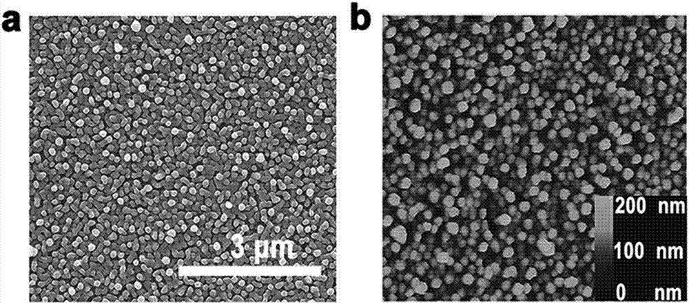
[0048] Soak the cleaned silicon chip in 10wt% hydrofluoric acid for 20 minutes, let it carry out the hydrosilylation reaction, and make the surface of the silicon chip form a Si-H bond, then place the processed silicon chip in a petri dish, with the shiny side facing Then put it into a mixed solution of 1M silver nitrate and 40wt% hydrogen fluoride (volume ratio = 1:50) for reduction reaction, the silver ions will be reduced by Si-H bonds, and a uniform layer of raw material will be formed on the surface o...
Embodiment 2
[0052] Take 0.5×0.5cm 2 Put 3 to 6 single silicon wafers of different sizes into a clean beaker and use deionized water and acetone to sonicate for 15 minutes respectively in an ultrasonic instrument to obtain silicon wafers with a clean surface for use. Then soak the silicon wafer in a mixed solution of 40 mL of sulfuric acid and hydrogen peroxide for 30 minutes to remove insoluble impurities therein, and finally clean the silicon wafer with deionized water for later use.
[0053] Soak the cleaned silicon chip in 20wt% hydrofluoric acid for 20 minutes, let it carry out the hydrosilylation reaction, and make the surface of the silicon chip form a Si-H bond, then place the processed silicon chip in a petri dish, with the shiny side facing Then put it into a mixed solution of 1M silver nitrate and 40wt% hydrogen fluoride (volume ratio = 1:50) for reduction reaction, the silver ions will be reduced by Si-H bonds, and a uniform layer of raw material will be formed on the surface o...
PUM
| Property | Measurement | Unit |
|---|---|---|
| size | aaaaa | aaaaa |
Abstract
Description
Claims
Application Information