Preparation method for quasi-vertical-structured GaN-based schottky diode

A Schottky diode, vertical structure technology, used in semiconductor/solid-state device manufacturing, electrical components, circuits, etc., to reduce expansion resistance, solve current crowding, and small ohmic contact distances

Inactive Publication Date: 2017-09-15
THE 13TH RES INST OF CHINA ELECTRONICS TECH GRP CORP
View PDF3 Cites 13 Cited by
  • Summary
  • Abstract
  • Description
  • Claims
  • Application Information

AI Technical Summary

Problems solved by technology

However, there is no GaN Schottky diode device with a quasi-vertical structure based on substrate replacement technology

Method used


Image

  • Preparation method for quasi-vertical-structured GaN-based schottky diode
  • Preparation method for quasi-vertical-structured GaN-based schottky diode
  • Preparation method for quasi-vertical-structured GaN-based schottky diode

Examples


Embodiment Construction

[0022] The present invention will be further described in detail below in conjunction with the accompanying drawings and specific embodiments.

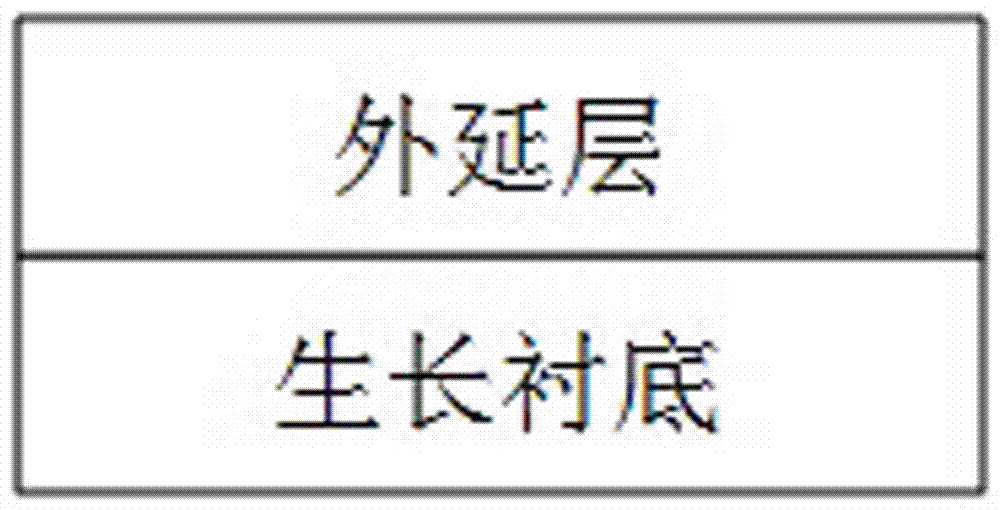
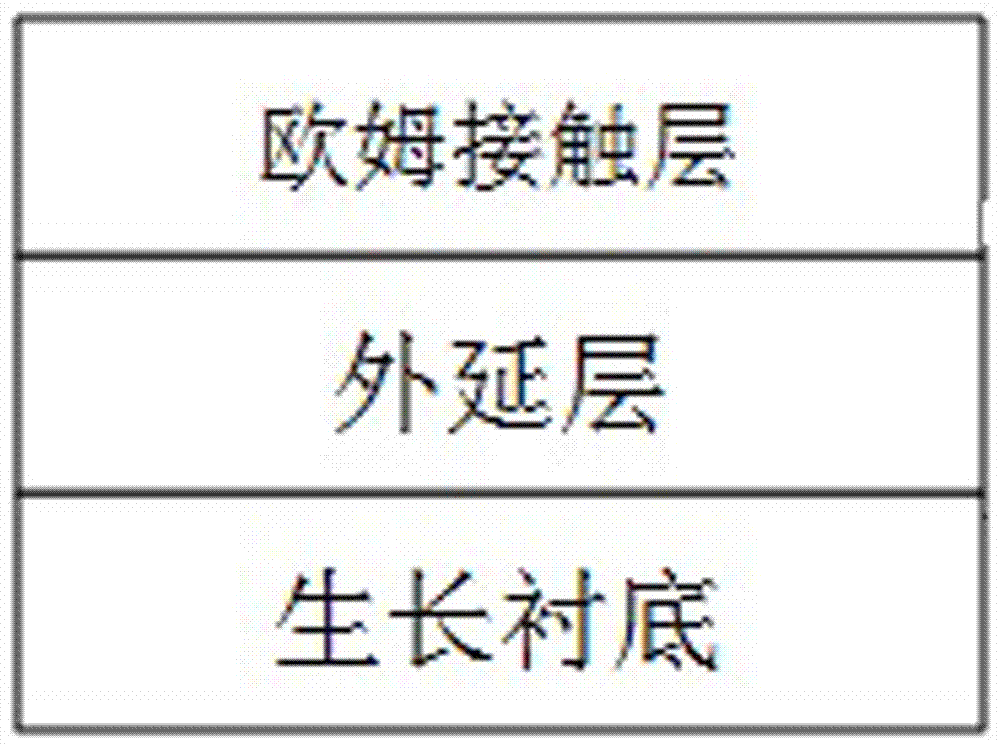
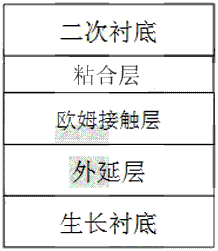
[0023] For the preparation method of the GaN-based Schottky diode with quasi-vertical structure provided by the present invention, please refer to Figure 1-Figure 5 , epitaxially growing a highly doped N-type GaN layer on the growth substrate; epitaxially growing a highly doped N+ GaN layer on the N-type GaN layer; making an ohmic contact on the N+ GaN layer, such as figure 2 As shown; Schottky contacts are formed on the N-layer, and the Schottky contacts are introduced to the anode through an air bridge, such as Figure 5 shown.

[0024] The technical solution further adopted by the present invention is that the doping elements of the highly doped N-type GaN layer epitaxially grown on the growth substrate are group IV elements, and the doping concentration is 10 16 / cm 3 magnitude to 10 19 / cm 3 Between magnitudes; the doping ...


PUM


Abstract

The invention discloses a preparation method for a quasi-vertical-structured GaN-based schottky diode, and belongs to the technical field of a semiconductor device. A highly-doped N-type GaN layer is grown on a growth substrate in an epitaxial way; a highly-doped N+ GaN layer is grown on the N-type GaN layer in an epitaxial way; ohmic contact is formed on the N+ GaN layer; and schottky contact is formed on an N- layer, and schottky contact is led to a positive electrode through an air bridge. By virtue of the preparation method, the series resistance of the device can be lowered, working frequency can be improved, and the problem of current crowding can be solved.

Description

technical field [0001] The invention belongs to the technical field of semiconductor devices, in particular to a preparation method of a GaN-based Schottky diode with a quasi-vertical structure. Background technique [0002] Schottky frequency doubler diode devices based on traditional semiconductor materials such as Si and GaAs are limited by the properties of the material itself, so it is difficult to further improve the corresponding indicators such as power and breakdown voltage. In recent years, a new generation of wide-bandgap semiconductor materials represented by group III nitrides has developed rapidly, with superior material properties such as wide band gap, high saturation electron drift velocity, high breakdown field strength and high thermal conductivity. The field of wave high-power electronic devices has great potential for development. Research on GaN-based Schottky diode millimeter wave and submillimeter wave frequency multiplier devices is currently a hot ...

Claims


Application Information

Patent Timeline
Patent Type & Authority Applications(China)
IPC IPC(8): H01L21/329
CPCH01L29/66143
Inventor 梁士雄王俊龙张立森杨大宝徐鹏赵向阳房玉龙冯志红
Owner THE 13TH RES INST OF CHINA ELECTRONICS TECH GRP CORP
Why Eureka
Try Eureka