
Oscillation circuit, booster circuit, and semiconductor device

An oscillating circuit and circuit technology, which is applied to logic circuits, logic circuits generating pulses, electrical pulse generator circuits, etc. Effect

Active Publication Date: 2017-09-26
SII SEMICONDUCTOR CORP
View PDF18 Cites 3 Cited by
  • Summary
  • Abstract
  • Description
  • Claims
  • Application Information

AI Technical Summary

Problems solved by technology

As a result, there is a problem that current consumption / power consumption will increase significantly

Method used


Image

  • Oscillation circuit, booster circuit, and semiconductor device
  • Oscillation circuit, booster circuit, and semiconductor device
  • Oscillation circuit, booster circuit, and semiconductor device

Examples


Embodiment Construction

[0032] Hereinafter, embodiments of the present invention will be described with reference to the drawings.

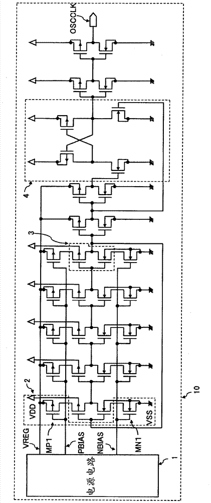
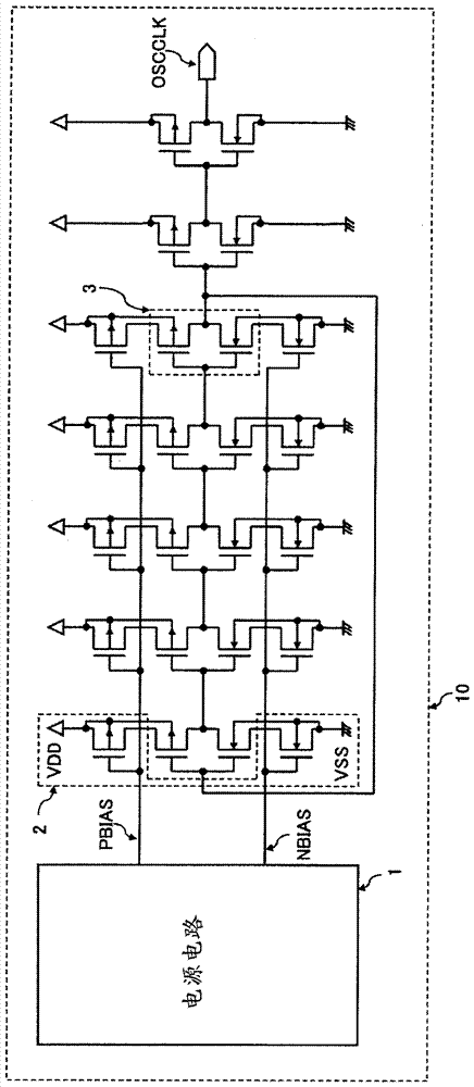
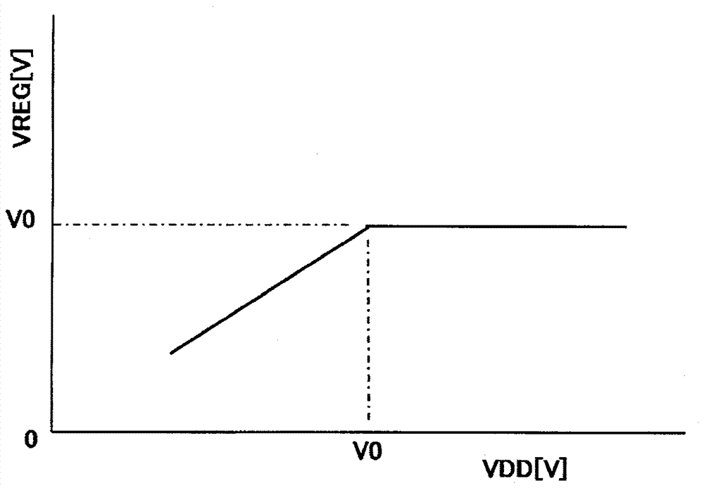
[0033] figure 1 It is a circuit diagram showing an example of the oscillation circuit 10 of this embodiment. It is a ring oscillator circuit formed by cascade-connecting inverter circuits 3 composed of PMOS transistors and NMOS transistors connected in series in an odd number of stages. The constant current elements 2 are respectively connected to the inverter circuits 3 . Each constant current element 2 is connected to the power supply circuit 1 . The substrate of the PMOS transistor of the inverter circuit 3 is connected to the power supply voltage VDD. The source of the PMOS transistor of the inverter circuit 3 is connected to the drain of the PMOS transistor MP1 that is the first constant current element that controls the supply current. The gate of the PMOS transistor MP1 is input with the bias voltage PBIAS output from the power supply circuit 1 , the source ...


PUM


Abstract

Provided are an oscillation circuit, a booster circuit, and a semiconductor device capable of reducing power consumption when a power supply voltage is high. In a ring oscillator circuit which is the oscillation circuit, a PMOS transistor in each of inverter circuits has a substrate connected to a first power supply voltage, and a source connected to a drain of a PMOS transistor, which is a first constant current element configured to control a supply current to the inverter circuit, and the PMOS transistor, which is the first constant current element, has a source connected to a second power supply voltage VREG, which serves as a constant voltage when the first power supply voltage is at a predetermined voltage or higher.

Description

technical field [0001] The present invention relates to an oscillation circuit capable of reducing power consumption at high supply voltages. Background technique [0002] In a nonvolatile memory such as an EEPROM in which data can be electrically erased / written / read, it is necessary to apply a high voltage equal to or higher than the power supply voltage VDD to a selected memory cell when erasing / writing operations are performed. The desired high voltage is generated using a charge pump circuit that boosts the input voltage. [0003] The output current of the booster circuit using the charge pump circuit is represented by the following equation (1). [0004] [0005] Here, TCLK is the oscillation period of the clock signal of the oscillation circuit, fCLK is the oscillation frequency of the output clock signal of the oscillation circuit, CCP is the capacitor capacitance of the charge pump circuit, and VCLK is the amplitude of the clock signal (= power supply voltage VDD...

Claims


Application Information

Patent Timeline
Patent Type & Authority Applications(China)
IPC IPC(8): H03K3/03H03K3/012
CPCH03K3/012H03K3/0315G11C5/145H02M3/073H03K3/011G11C5/147H03K3/354H03K19/018521H03K19/018507
Inventor 村田正哉
Owner SII SEMICONDUCTOR CORP
Learn More