Laminated electric field modulation high-voltage MOSFET structure and method for manufacturing same

A manufacturing method and electric field technology, which are applied in the manufacturing of circuits, electrical components, semiconductor/solid-state devices, etc., can solve the problems of reducing the thickness of epitaxial layers, breaking blocking voltage, reducing on-resistance, etc., and reducing the difficulty of processing technology. , the effect of increasing blocking voltage and reducing on-resistance

Inactive Publication Date: 2017-09-29
GLOBAL ENERGY INTERCONNECTION RES INST CO LTD
View PDF4 Cites 5 Cited by
  • Summary
  • Abstract
  • Description
  • Claims
  • Application Information

AI Technical Summary

Problems solved by technology

[0003] The blocking voltage and forward conduction resistance of the traditional power semiconductor device MOSFET have mutual constraints. Increasing the thickness of the epitaxial layer and reducing the doping concentration can increase the blocking voltage, but at the s...

Method used


Image

  • Laminated electric field modulation high-voltage MOSFET structure and method for manufacturing same
  • Laminated electric field modulation high-voltage MOSFET structure and method for manufacturing same
  • Laminated electric field modulation high-voltage MOSFET structure and method for manufacturing same

Examples


Embodiment Construction

[0052] The technical solution of the present invention will be clearly and completely described below in conjunction with the accompanying drawings and specific embodiments. Obviously, the described embodiments are only some of the embodiments of the present invention, not all of them. Based on the embodiments of the present invention, all other embodiments obtained by persons of ordinary skill in the art without making creative efforts belong to the protection scope of the present invention.

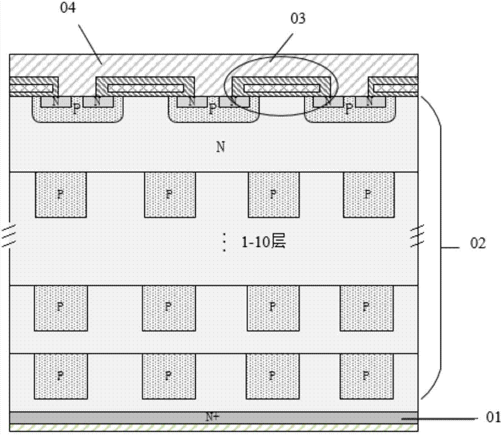
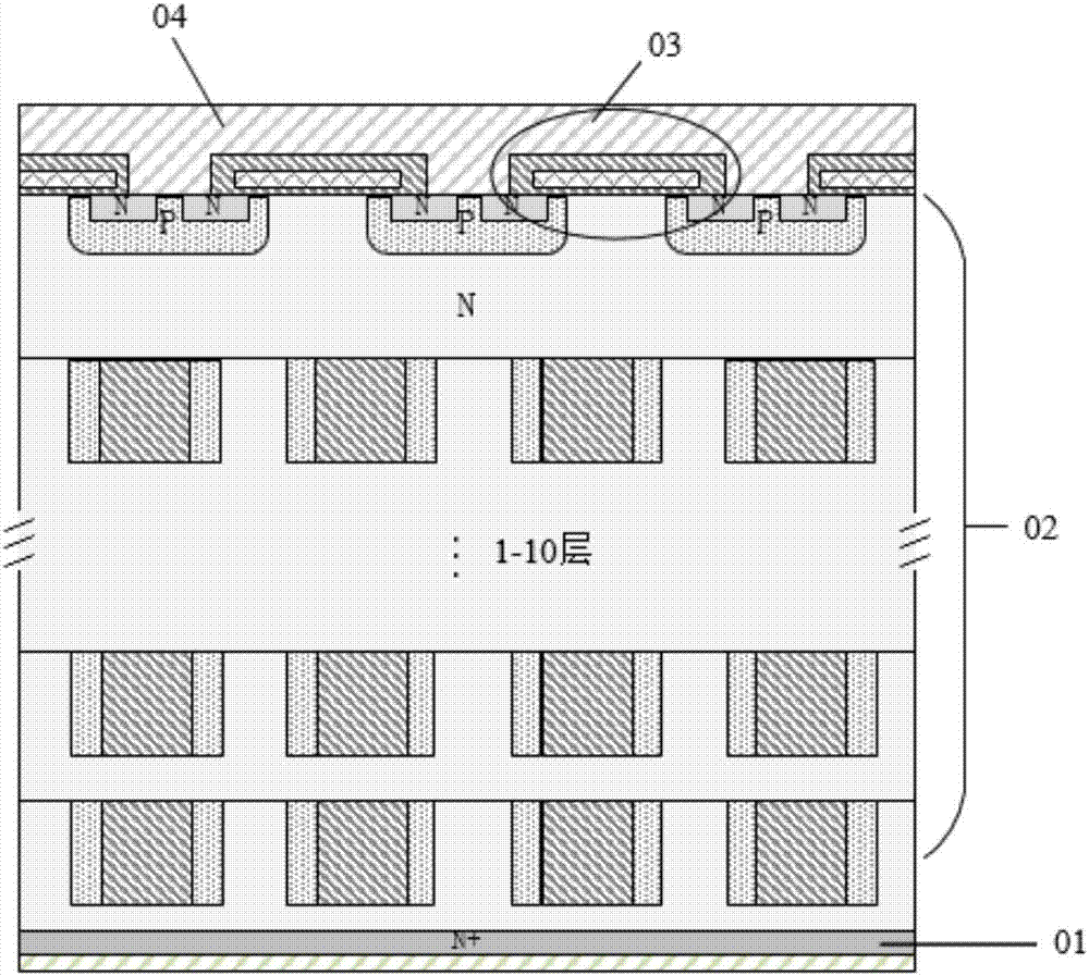
[0053]The present invention takes the silicon carbide material of the n-type substrate as an example to manufacture a stacked electric field modulation n-channel MOSFET device, wherein another important structure of the MOSFET device is a double-diffusion metal-oxide-semiconductor structure. Similarly, p-channel MOSFET devices and trench MOSFETs are also applicable to the method of the embodiment of the present invention.

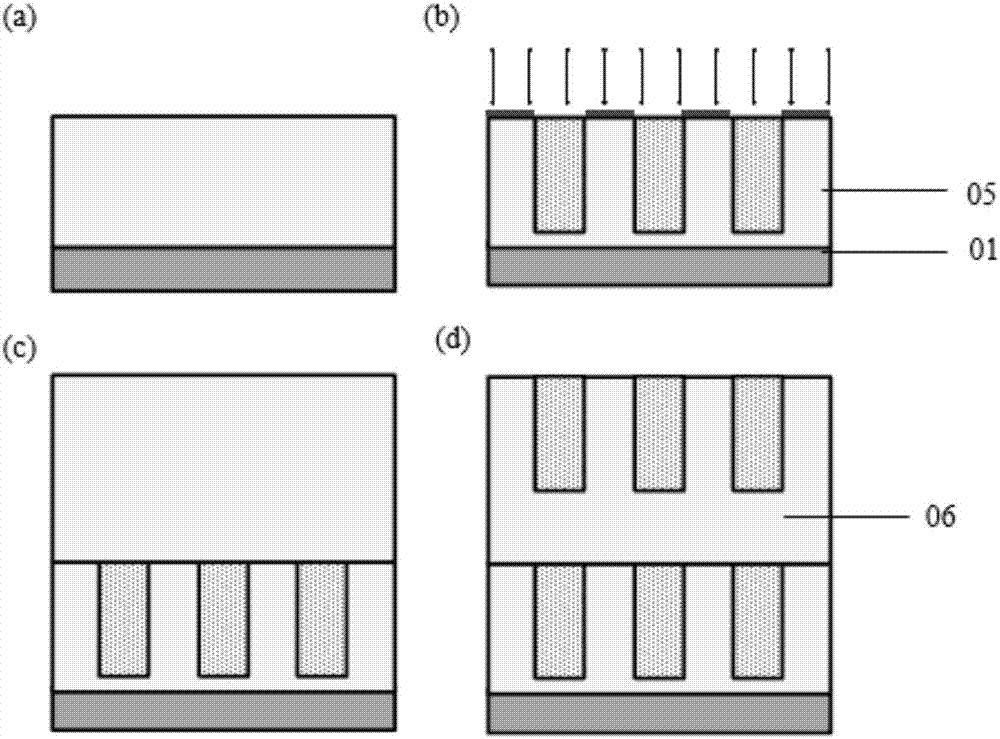
[0054] A method for manufacturing a stacked electric field modu...


PUM

PropertyMeasurementUnit
Thicknessaaaaaaaaaa
Thicknessaaaaaaaaaa

Abstract

The invention provides a laminated electric field modulation high-voltage MOSFET structure and a method for manufacturing the same. The MOSFET structure includes a semiconductor substrate provided with the epitaxial layer of a laminated electric field modulation structure and the metal-oxide-semiconductor (MOS) structure on the laminated electric field modulation. The laminated electric field modulation is an N/P/N/P structure composed of alternate n-type semiconductors and p-type semiconductors. The N/P structure and the semiconductor substrate have the same material. The N-doped region and the P-doped region in the layer are aligned to each other. The invention provides different methods for manufacturing the electric field modulation structure, including a high-energy ion implantation method, an etching deep groove and filling method, and an etching deep groove and sidewall ion implantation method, thereby laying the foundation for the fabrication of a device. The MOSFET obtained by the technical scheme in the invention not only inherits advantages of increasing blocking voltage and decreasing on-resistance of a traditional semi-super junction structure, but also reduces the difficulty of processing technology of each electric field modulation structure layer.

Description

technical field [0001] The invention relates to a MOSFET structure, in particular to a laminated electric field modulation high-voltage MOSFET structure and a manufacturing method thereof. Background technique [0002] Metal-Oxide Semiconductor Field-Effect Transistor, referred to as Metal-Oxide-Semiconductor Field-Effect Transistor (MOSFET), is a field-effect transistor (field-effect transistor) that can be widely used in high-voltage and high-power fields. . [0003] The blocking voltage and forward conduction resistance of the traditional power semiconductor device MOSFET have mutual constraints. Increasing the thickness of the epitaxial layer and reducing the doping concentration can increase the blocking voltage, but at the same time increase the conduction resistance, thereby reducing the forward conduction resistance. To the current density, on the contrary, reducing the thickness of the epitaxial layer and increasing the doping concentration can reduce the on-resist...

Claims


Application Information

Patent Timeline
IPC IPC(8): H01L29/78H01L29/06H01L21/336
CPCH01L29/0634H01L29/66674H01L29/7801
Inventor 杨霏潘艳李玲郑柳查祎英赵岩田丽欣
Owner GLOBAL ENERGY INTERCONNECTION RES INST CO LTD
Why Eureka
Try Eureka