Novel semiconductor photomultiplier device

A photoelectric multiplication and semiconductor technology, applied in semiconductor devices, semiconductor/solid-state device manufacturing, electric solid-state devices, etc., can solve the problems of high optical crosstalk probability of devices, loss of signal detection ability, annihilation of signals, etc., to reduce optical crosstalk and improve Single-photon resolution ability, effect of reducing background noise

Active Publication Date: 2017-10-20
湖北京邦科技有限公司
View PDF7 Cites 4 Cited by
  • Summary
  • Abstract
  • Description
  • Claims
  • Application Information

AI Technical Summary

Problems solved by technology

These three types of optical crosstalk exist and occur simultaneously in ordinary semiconductor photomultiplier devices, and the superposition of the three will lead to a higher probability of optical crosstalk in the device
Optical crosstalk belongs to the backgro

Method used


Image

  • Novel semiconductor photomultiplier device
  • Novel semiconductor photomultiplier device
  • Novel semiconductor photomultiplier device

Examples


Example Embodiment

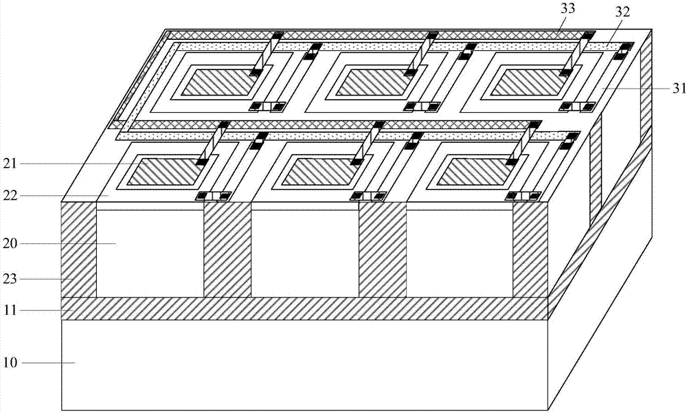
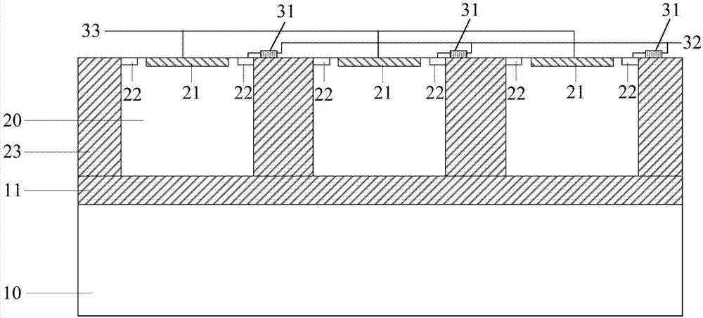
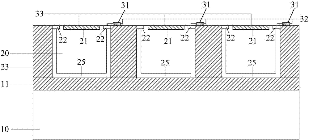
[0026] as attached figure 1 As shown, a novel semiconductor photomultiplier device disclosed in the present invention is characterized by comprising: an SOI substrate 10; a semiconductor epitaxial layer 20 of a first doping type located on the SOI substrate layer 10; N (in this embodiment, N is 6) photodiodes in the semiconductor epitaxial layer of the first doping type; and N high-resistance resistors 31 set corresponding to the N photodiodes one by one; Each of the photodiodes is electrically connected to a high-resistance resistor 31, and the ends of the photodiodes that are not connected to the high-resistance resistor 31 are electrically connected to each other, that is, through the figure 1 The photodiode interconnect lines 33 shown are connected to each other; the ends of each of the high-resistance resistors 31 that are not connected to the photodiode are electrically connected to each other, that is, through the figure 1 Resistive interconnect lines 32 are shown conn...


PUM

PropertyMeasurementUnit
Sheet resistanceaaaaaaaaaa

Abstract

A novel semiconductor photomultiplier device includes an epitaxial photodiode array over an SOI substrate, a deep trench dielectric layer that completely isolates each photodiode, a high resistance resistor in series connection with each of the photodiodes, and metal interconnection lines for the interconnection of the high resistance resistor and the photodiodes. The benefit effect is that the deep trench dielectric layer and the SOI substrate completely isolate each of the photodiodes from the other adjacent photodiodes, prevent direct optical crosstalk and delay optical crosstalk, and reduce the influence of secondary photons on the adjacent photodiodes, so as to significantly reduce the overall optical crosstalk of the device, and significantly enhance the single-photon resolution.

Description

technical field [0001] The invention relates to the fields of optoelectronics and microelectronics, in particular to a semiconductor photomultiplier device for photon detection. Background technique [0002] The semiconductor photomultiplier is a new type of semiconductor device that uses the semiconductor avalanche multiplication mechanism to detect photons. It is an array detection structure composed of multiple detection units arranged in parallel. All detection units share one electrode for signal output. The detection unit is composed of an avalanche photodiode series quenching resistor working in Geiger mode. When photons are incident into the diode and absorbed, electron-hole pairs will be generated in the photosensitive region of the avalanche photodiode. Due to the high electric field in the photosensitive area of ​​the avalanche photodiode, the drifting electrons will generate a large number of electron-hole pairs in this high electric field through avalanche mult...

Claims


Application Information

Patent Timeline
IPC IPC(8): H01L31/102H01L27/142H01L27/144H01L21/762
CPCY02E10/50H01L31/102H01L21/76224H01L21/7624H01L27/142H01L27/1446
Inventor 徐青王麟N·达申佐谢庆国
Owner 湖北京邦科技有限公司
Why Eureka
Try Eureka