Dry film developing technique used for high density circuit of printed circuit board

A printed circuit board and dry film technology, which is applied in printed circuits, printed circuit manufacturing, photosensitive material processing, etc., can solve problems such as the inability to ensure the electrical performance requirements of high-density circuits, the inability of the development process to meet the needs of industrialization, and the easy generation of development burrs. , to achieve the effect of low cost, low price and no pollution in the production process

Inactive Publication Date: 2017-10-20
东莞市斯坦得电子材料有限公司
View PDF6 Cites 1 Cited by
  • Summary
  • Abstract
  • Description
  • Claims
  • Application Information

AI Technical Summary

Problems solved by technology

[0002] The dry film development process of printed circuit boards is traditionally carried out with sodium carbonate solution, and the process has the following shortcomings: 1) It can only develop circuit boards with a line width and line spacing > 0.15mm, but cannot develop circuit boards with a line width and line spacing ≤ 0.1mm Circuit board; 2) easy to produce developing burrs; 3) easy to produce line sawtooth; 4) cannot ensure the electrical performance requirements of high-density lines (line width and line spacing ≤ 0.1mm), with the increasing miniaturization and multi-function of electronic products, The density of printed circuits is getting higher and higher (line width and line spacing are getting smaller and smaller), and the traditional sodium carbonate system development process cannot meet the needs of industrialization

Method used


Image

  • Dry film developing technique used for high density circuit of printed circuit board
  • Dry film developing technique used for high density circuit of printed circuit board
  • Dry film developing technique used for high density circuit of printed circuit board

Examples


Embodiment 1

[0014] Drain the working solution of the dry film developing tank first, rinse it with tap water, and continue to wash it with deionized water for 30 minutes. Prepare 1 liter of potassium carbonate aqueous solution, wherein potassium carbonate is 20 grams. Add 1 liter of potassium carbonate aqueous solution to the dry film developing tank, heat to 28°C, the pH of the potassium carbonate aqueous solution is 10.5, and the specific gravity is 1.02g / cm 3 . Start the circulating filter pump, put the exposed dry film board of the printed circuit to be developed into the potassium carbonate aqueous solution, spray and soak for 1min; then take out the developed printed circuit board, wash it with tap water for 1min; finally dry it with hot air for 0.4min , into the pattern plating process or inner layer etching process.

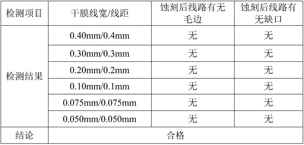
[0015] It can be seen from the experimental results that this process makes the dry film of the high-density circuit flush with the line edge after development, wi...

Embodiment 2

[0019] Drain the working solution of the dry film developing tank first, rinse it with tap water, and continue to wash it with deionized water for 30 minutes. Prepare 1 liter of potassium carbonate aqueous solution, wherein potassium carbonate is 25 grams. Add 1 liter of potassium carbonate aqueous solution to the dry film developing tank, heat to 30°C, the pH of the potassium carbonate aqueous solution is 12, and the specific gravity is 1.03g / cm 3 . Start the circulating filter pump, put the exposed dry film board of the printed circuit to be developed into the potassium carbonate aqueous solution, spray and soak for 1.5min; then take out the developed printed circuit board, wash it with tap water for 1.5min; finally dry it with hot air 0.5min, transfer to pattern electroplating process or inner layer etching process.

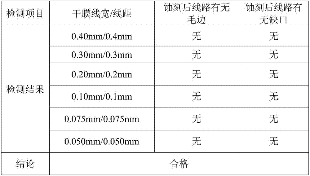
[0020] It can be seen from the experimental results that this process makes the dry film of the high-density circuit flush with the line edge after developm...

Embodiment 3

[0024] Drain the working solution of the dry film developing tank first, rinse it with tap water, and continue to wash it with deionized water for 30 minutes. Prepare 1 liter of potassium carbonate aqueous solution, wherein potassium carbonate is 30 grams. Add 1 liter of potassium carbonate aqueous solution to the dry film developing tank, heat to 32°C, the pH of the potassium carbonate aqueous solution is 13.5, and the specific gravity is 1.05g / cm 3 . Start the circulating filter pump, put the exposed dry film board of the printed circuit to be developed into the dry film developer, spray and soak for 2 minutes; then take out the developed printed circuit board and wash it with tap water for 2 minutes; finally dry it with hot air for 0.6 min, transfer to pattern electroplating process or inner layer etching process.

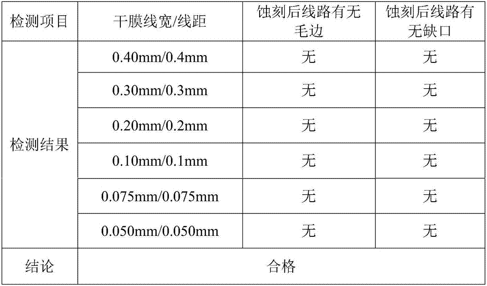
[0025] It can be seen from the experimental results that this process makes the dry film of the high-density circuit flush with the line edge after developmen...


PUM

PropertyMeasurementUnit
Proportionaaaaaaaaaa

Abstract

The invention provides a dry film developing technique used for a high density circuit of a printed circuit board. The dry film developing technique includes steps of discharging working liquid in a dry film developing tank completely, flushing the dry film developing tank with water and using deionized water for cyclic washing continually; adding aqueous solution of a dry film developing agent into the dry film developing tank, heating to 28 to 32 DEG C; starting a circulating filtration pump, placing the to-be-developed printed circuit board into the aqueous solution of the dry film developing agent, spraying and soaking; finally taking the printed circuit board out and cleaning with running water, drying with hot air and turning to a graphic electroplating working procedure or an inner layer etching working procedure. By adopting the technical provided by the invention, development of high density circuits with line width and line space smaller than or equal to 0.01 mm can be realized. Besides, edge levelness of graphic circuits after development is realized and rough edges or line jags are avoided, so that the electrical property of the printed circuit board is improved. The production process is pollution free and industrial production is facilitated.

Description

technical field [0001] The invention belongs to the technical field of printed circuit board processing, and in particular relates to a dry film development process for high-density circuits of printed circuit boards. Background technique [0002] The dry film development process of printed circuit boards is traditionally carried out with sodium carbonate solution, and the process has the following shortcomings: 1) It can only develop circuit boards with a line width and line spacing > 0.15mm, but cannot develop circuit boards with a line width and line spacing ≤ 0.1mm Circuit board; 2) easy to produce developing burrs; 3) easy to produce line sawtooth; 4) cannot ensure the electrical performance requirements of high-density lines (line width and line spacing ≤ 0.1mm), with the increasing miniaturization and multi-function of electronic products, The density of printed circuits is getting higher and higher (line width and line spacing are getting smaller and smaller), and...

Claims


Application Information

Patent Timeline
IPC IPC(8): H05K3/06G03F7/30
CPCH05K3/06G03F7/30H05K2203/052
Inventor 束学习
Owner 东莞市斯坦得电子材料有限公司
Why Eureka
Try Eureka