Silicon carbide power device terminal and manufacturing method thereof

A technology for power devices and manufacturing methods, which is applied in semiconductor/solid-state device manufacturing, semiconductor devices, electrical components, etc., can solve problems such as interface instability, increase current, affect the distribution of electric field on the surface of the device, and improve the charge resistance of the device. and reliability, ensure device withstand voltage, and improve the effect of surface electric field distribution

Inactive Publication Date: 2017-10-24
INST OF MICROELECTRONICS CHINESE ACAD OF SCI
View PDF3 Cites 3 Cited by
  • Summary
  • Abstract
  • Description
  • Claims
  • Application Information

AI Technical Summary

Problems solved by technology

The existing terminal structure design is complex, and the terminal occupies a large total area of ​​the chip, which is not conducive to increasing the current, and is sensitive to surface charges, and is easily

Method used


Image

  • Silicon carbide power device terminal and manufacturing method thereof
  • Silicon carbide power device terminal and manufacturing method thereof

Examples


Example Embodiment

[0019] Some embodiments of the present invention will be described more fully in the following with reference to the accompanying drawings, and some but not all of the embodiments will be shown. In fact, various embodiments of the present invention can be implemented in many different forms, and should not be construed as being limited to the embodiments described in this number; relatively, the provision of these embodiments enables the present invention to meet applicable legal requirements.

[0020] In order to make the objectives, technical solutions, and advantages of the present invention clearer, the following further describes the present invention in detail in conjunction with specific embodiments and with reference to the accompanying drawings.
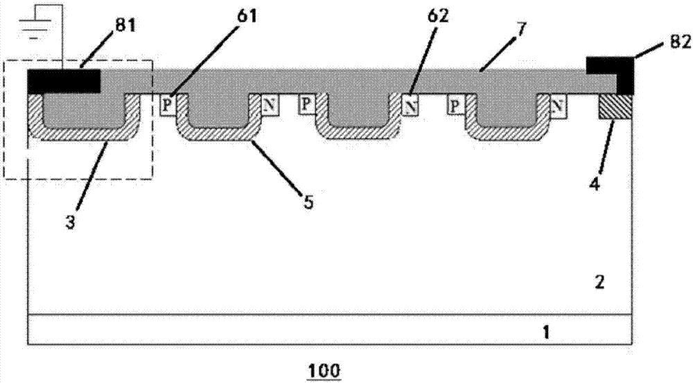
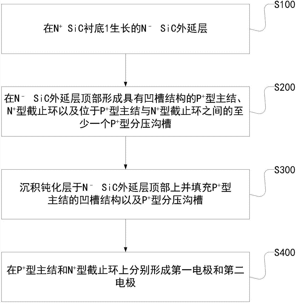
[0021] The embodiment of the present invention provides a silicon carbide power device terminal, including: a first heavily doped type or a second heavily doped type SiC substrate; grown on a first heavily doped type or a second h...


PUM


Abstract

The invention discloses a silicon carbide powder device terminal and a manufacturing method thereof. The silicon carbide power device terminal comprises a first heavily-doped or second heavily-doped SiC substrate, a first lightly-doped SiC epitaxial layer, a second heavily-doped main junction, a first doped stop ring and at least one second heavily-doped partial pressure groove, wherein the first lightly-doped SiC epitaxial layer grows on the first heavily-doped or second heavily-doped SiC substrate; the second heavily-doped main junction and the first doped stop ring are provided with groove structures, and formed on the top of the first lightly-doped SiC epitaxial layer; and the at least one second heavily-doped partial pressure groove is formed between the second heavily-doped main junction and the first doped stop ring.

Description

technical field [0001] The invention relates to the field of semiconductor power devices, in particular to a silicon carbide power device terminal and a manufacturing method thereof. Background technique [0002] The third-generation semiconductor material silicon carbide (SiC) has the advantages of large band gap, high critical breakdown field strength, high thermal conductivity and high electron saturation rate, and is very suitable for making high-voltage, high-temperature, high-frequency, high-power semiconductor devices. Silicon carbide power devices (SiC diodes, SiC MOSFETs, etc.), as a new generation of high-efficiency power electronic devices, have become the most important development direction of power electronics technology, and have important applications in new energy vehicles, rail transit, locomotive traction, smart grid and other fields Prospects and development, and an important condition for silicon carbide power devices to have high withstand voltage chara...

Claims


Application Information

Patent Timeline
IPC IPC(8): H01L29/861H01L29/06H01L21/329
CPCH01L29/0623H01L29/0661H01L29/6606H01L29/8611
Inventor 田晓丽白云杨成樾汤益丹陈宏刘新宇
Owner INST OF MICROELECTRONICS CHINESE ACAD OF SCI
Why Eureka
Try Eureka