A soi power ldmos device with junction field plate

A junction field plate and device technology, applied in semiconductor devices, electrical components, diodes, etc., can solve the problems of large leakage current of resistive field plates and increase of device breakdown voltage, so as to reduce leakage current, reduce on-resistance, The effect of increased doping concentration

Inactive Publication Date: 2015-10-21
UNIV OF ELECTRONICS SCI & TECH OF CHINA +1
View PDF4 Cites 0 Cited by
  • Summary
  • Abstract
  • Description
  • Claims
  • Application Information

AI Technical Summary

Problems solved by technology

The advantage of the resistive field plate of semi-insulating polysilicon is that it effectively eliminates the high electric field at the end of the ordinary metal field plate, making the electric field intensity distribution along the surface of the drift region relatively flat, and the breakdown voltage of the device is greatly improved; however, the resistive field plate There is a disadvantage of large leakage current

Method used


Image

  • A soi power ldmos device with junction field plate
  • A soi power ldmos device with junction field plate
  • A soi power ldmos device with junction field plate

Examples


Embodiment 1

[0036] Fig. 6(a) shows a cross-sectional view of a half-cell structure of a JFP SOI LDMOS device using a trench gate structure. The devices in this example include:

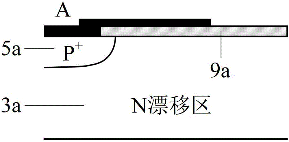
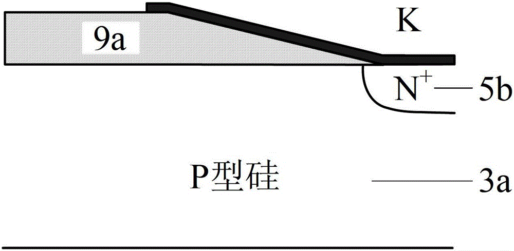
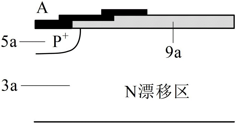
[0037] It includes a substrate layer 1, a dielectric buried layer 2, and an active layer 3 vertically from bottom to top; the active layer 3 is a doped semiconductor of the first conductivity type, and has: a drain region 7c of a doped semiconductor of the first conductivity type , a source region 7b of a semiconductor doped with a first conductivity type, a body region 6 of a semiconductor doped with a second conductivity type, and a body contact region 7a of a semiconductor doped with a second conductivity type. The second conductivity type doped semiconductor body region 6 is located on one side of the surface of the active layer 3, the first conductivity type doped semiconductor source region 7b is adjacent to the second conductivity type doped semiconductor body contact region 7a and Located on the surface ...

Embodiment 2

[0042] Figure 7 A schematic diagram of half a cell structure of the JFP SOI LDMOS device of this embodiment is shown. Compared with Embodiment 1, the device of this embodiment inserts the first conductivity type doped semiconductor buffer zone 12 between the high resistance region 11 and the N-type ohmic contact region 10b in the junction field plate, and other structures are the same as Embodiment 1. The doping concentration of the first conductivity type doped semiconductor buffer area 12 is lower than the concentration of the ohmic contact of the junction field plate, so as to reduce the electric field peak at the PN junction of the field plate, thereby preventing the device from being placed at the PN junction of the field plate Early breakdown. Therefore, compared with the device of Example 1, the withstand voltage of the device in this example is relatively high.

Embodiment 3

[0044] Compared with Example 1, the device of this example injects a layer of thinner (for example, about 0.5um) buffer layer 13 at the interface between the active layer and the buried dielectric layer, such as Figure 8 shown. For N-channel JFP SOI LDMOS devices, the buffer layer is N-type doped; at this time, the buffer layer 13 not only serves as a transmission channel for high current density, but also increases the vertical electric field at the interface between the active layer and the dielectric buried layer, thereby The electric field distribution in the dielectric buried layer is improved, which is beneficial to the improvement of the vertical withstand voltage of the device. The device in this example is only applicable to N-channel JFP SOI LDMOS devices.


PUM


Abstract

The invention discloses an SOI power LDMOS device provided with a junction type field plate structure, and belongs to the technical field of power semiconductor devices. According to the JFP SOI LDMOS device, a PN junction is adopted as a field plate, and a high-K medium is used as a field plate medium. On one hand, a PN junction electric field of the junction type field plate modulates the electric field on the surface of the device to improve the electric field distribution of the device and enhance the pressure resistance of the device; on the other hand, in a reverse blocking state, the junction type field plate assists in exhausting a drift region of the device to enable the doping density of the drift region of the device to be increased substantially, so that on-resistance is lowered; the high-K medium is used as a field dielectric layer so that the on-resistance and static power consumption can be lowered more beneficially. Compared with a conventional metal field plate, the junction type field plate technology also effectively avoids the defect that an electric field peak exists at the tail end of the field plate; compared with a polycrystalline resistance field plate, the junction type field plate has a PN junction potential barrier so that a high leakage current can be avoided. In addition, the SOI power LDMOS device provided with the junction type field plate structure also has good compatibility with SOI CMOS circuits.

Description

technical field [0001] The invention belongs to the field of power semiconductor devices, and relates to SOI (Silicon On Insulator, semiconductor on an insulating layer) lateral power device, in particular to a high-voltage and low-resistance SOI lateral power MOSFET (Metal Oxide Semiconductor Field Effect Transistor, Metal Oxide Semiconductor Field Effect Transistor) with a new terminal structure Oxide Semiconductor Field Effect Transistor) devices. Background technique [0002] Compared with power semiconductor devices with bulk silicon structure, power semiconductor devices with SOI structure have the advantages of small parasitic effect, small leakage current, high integration, strong radiation resistance and no SCR self-locking effect. Compared with VDMOS (Vertical Double-diffused MOSFET) devices, LDMOS (Lateral Double-diffused MOSFET) devices have higher switching speed, relatively low on-resistance, and easy integration. Therefore, SOI power LDMOS devices are widely ...

Claims


Application Information

Patent Timeline
Patent Type & Authority Patents(China)
IPC IPC(8): H01L29/78H01L29/423
CPCH01L29/7824H01L29/402H01L29/7825H01L29/7818H01L29/0692
Inventor 罗小蓉罗尹春范远航徐青魏杰范叶王骁玮周坤张彦辉尹超张波李肇基
Owner UNIV OF ELECTRONICS SCI & TECH OF CHINA
Why Eureka
Try Eureka