AlGaN heterojunction nano-pillar array light-emitting device and preparation method for the same

A technology of nano-pillar arrays and light-emitting devices, which is applied in semiconductor devices, electrical components, circuits, etc., can solve the problems of different chemical properties, poor flatness of AlGaN films, and high defect density, and achieves the effect of improving extraction efficiency and luminous efficiency.

Active Publication Date: 2017-10-24
NANJING UNIV
View PDF11 Cites 5 Cited by
  • Summary
  • Abstract
  • Description
  • Claims
  • Application Information

AI Technical Summary

Problems solved by technology

Due to poor flatness of AlGaN film, high defect density, and different chemical properties from InGaN / GaN, there are no relevant patent documents on the preparation of large-area AlGaN nano-column array structures with high Al composition

Method used


Image

  • AlGaN heterojunction nano-pillar array light-emitting device and preparation method for the same
  • AlGaN heterojunction nano-pillar array light-emitting device and preparation method for the same
  • AlGaN heterojunction nano-pillar array light-emitting device and preparation method for the same

Examples


Embodiment 1

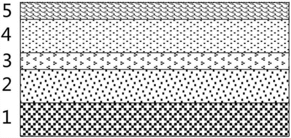
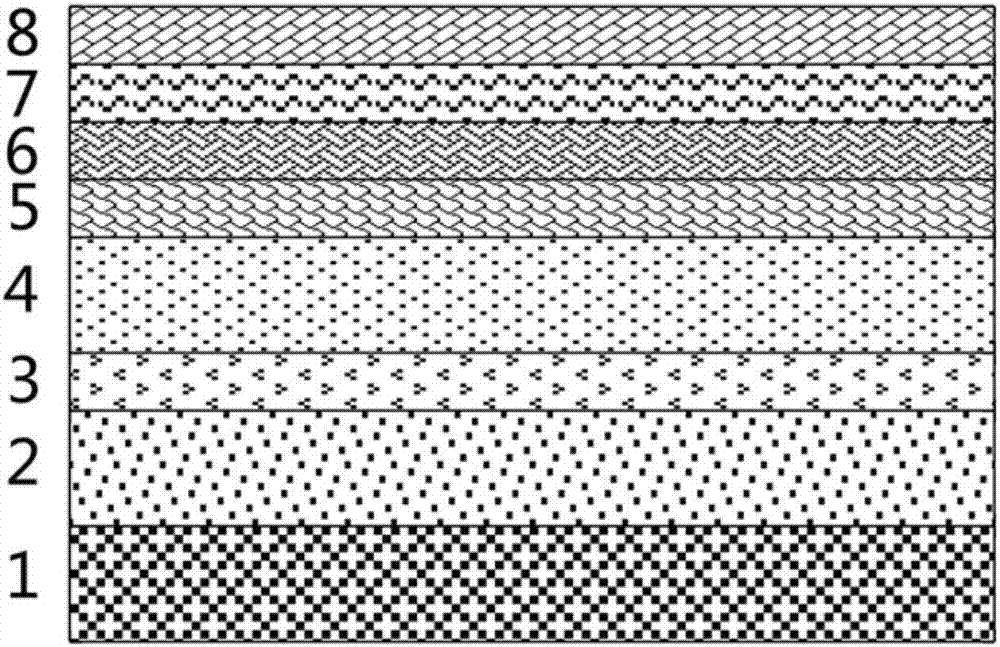
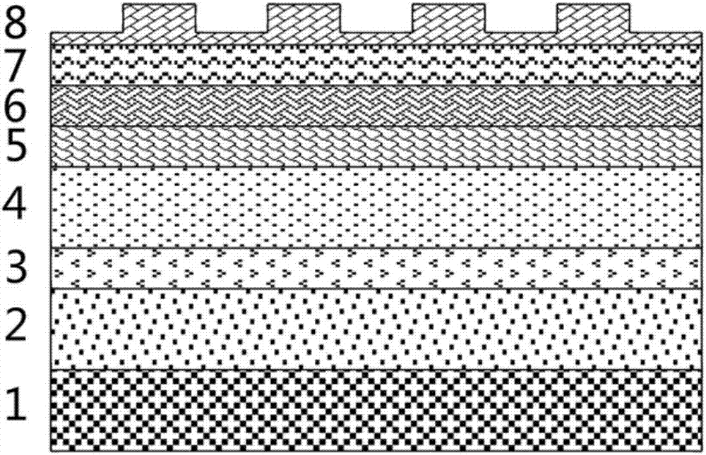
[0068] like Figure 1-10 Shown in, the preparation method of this AlGaN nanocolumn array structure, its step comprises:

[0069] 1) Select a GaN / AlN / AlGaN epitaxial substrate with x as 0.1, the thickness of the GaN buffer layer is 2μm, the thickness of the AlN insertion layer is 30nm, and the thickness of the AlGaN layer is 300nm-0.1μm, with acetone, isopropanol and deionized water After cleaning, dry it with high-purity nitrogen in a clean room, and grow a layer of high-temperature SiO on its surface by plasma-enhanced chemical vapor deposition. 2 layer with a thickness of 300nm;

[0070] 2) Spin-coat 200nm thick PMMA glue on SiO 2 layer surface, and then grow a layer of low-temperature SiO on the PMMA surface by plasma-enhanced chemical vapor deposition 2 The barrier layer has a thickness of 30nm, and then spin-coats a 30nm thick UV-curable adhesive on the surface of the barrier layer;

[0071] 3) Using UV-NIL technology, the pre-prepared and anti-adhesive treated soft t...

Embodiment 2

[0083] The steps of this embodiment are basically the same as those of Embodiment 1, the difference is that the Al composition x of the GaN / AlN / AlGaN epitaxial substrate is selected to be 0.18, the thickness of the AlGaN epitaxial layer is 1-1.5 μm, and the etching time of ICP is 10 minutes. The modification time of the corresponding inorganic alkali solution is 4min.

[0084] The prepared AlGaN nanocolumn array structure is as follows Figure 16 As shown in , its cathodofluorescence spectrum is shown in Figure 23 As shown in , the diameter of the nanocolumn array is 350 nm, the diameter of the AlxGa1-xN layer is 80 nm smaller than that of the AlN intercalation layer, the period is 700 nm, and the height is 1.1–1.6 μm.

Embodiment 3

[0086] The steps of this example are basically the same as those of Example 1, the difference is that the Al composition x of the GaN / AlN / AlGaN epitaxial substrate is selected as 0.3, the thickness of the AlGaN epitaxial layer is 0.5-1 μm, and the etching time of ICP is 12 minutes. The modification time of the inorganic alkali solution is 2min.

[0087]The diameter of the prepared AlGaN nanocolumn array is 300nm, the diameter of the AlxGa1-xN layer is 50nm smaller than that of the AlN insertion layer, the period is 600nm, and the height is 0.6-1.1μm. Its structure is as follows Figure 17 As shown in , its cathodofluorescence spectrum is shown in Figure 24 shown in .


PUM


Abstract

The present invention discloses an AlGaN heterojunction nano-pillar array light emitting device, whose structure comprises the following components that are sequentially arranged in the order from the bottom to the top: a substrate; a GaN buffer layer grown on the substrate; an AlN insertion layer grown on the GaN buffer layer; an AlxGa1-xN layer grown on the AlN insertion layer; and an etched nano-pillar array penetrating from the AlxGa1-xN layer, the AlN insertion layer and deeply into the GaN buffer layer. In the nano-pillar array, the diameter of the AlxGa1-xN layer is smaller than that of the AlN insertion layer. The invention also discloses a preparation method for the AlGaN heterojunction nano-pillar array light emitting device. According to the invention, through the use of a nano-pillar array structure of the invention, the stress in the heteroepitaxial film is released and the luminous efficiency of the device is increased; and through the change of the array structure parameters, the distribution of the light field can be adjusted, and the extraction efficiency for the ultraviolet light is increased. The utilization of the optimized three-layer UV flexible imprinting technology overcomes the defect caused by the surface roughness of the AlGaN epitaxial wafer; and the edge of the imprinted pattern is smooth and without serration, and the shape and the diameter of the nano-pillar array can be adjusted, and the structure can be transferred.

Description

technical field [0001] The patent of the invention relates to an AlGaN heterojunction nanocolumn array light-emitting device and a preparation method thereof, belonging to the field of semiconductor lighting and optoelectronic devices. Background technique [0002] After more than 20 years of development, high-efficiency, high-brightness blue LEDs based on GaN materials are becoming more and more mature. As the wavelength is further shortened, the luminescence enters the ultraviolet region. Ultraviolet light can have a strong interaction with biomolecules or chemical substances, and can be used in gas sensing, fluorescence excitation, UV curing, water purification, air disinfection and various microbial related equipment. Compared with traditional mercury lamps, UV LEDs are more robust, compact, environmentally friendly, have a long lifespan, do not require preheating, and can be switched on and off within nanoseconds, which has significant advantages. By adjusting the Al ...

Claims


Application Information

Patent Timeline
Patent Type & Authority Applications(China)
IPC IPC(8): H01L33/32H01L33/12H01L33/24H01L33/00
CPCH01L33/0029H01L33/0075H01L33/12H01L33/24H01L33/32
Inventor 刘斌戴姜平张荣陶涛谢自力陈敦军韩平施毅郑有炓
Owner NANJING UNIV
Why Eureka
Try Eureka