Inverted LED epitaxial wafer of GaAs-based armoring layer structure and manufacturing method of inverted LED epitaxial wafer

A technology of LED epitaxial wafers and roughened layers, which is applied to electrical components, circuits, semiconductor devices, etc., and can solve problems such as poor reliability and stability, and low brightness

Active Publication Date: 2017-11-03
Shandong Huaguang Optoelectronics Co. Ltd.
View PDF3 Cites 8 Cited by
  • Summary
  • Abstract
  • Description
  • Claims
  • Application Information

AI Technical Summary

Problems solved by technology

[0006] However, the traditional GaAs LED flip chip has the di

Method used


Image

  • Inverted LED epitaxial wafer of GaAs-based armoring layer structure and manufacturing method of inverted LED epitaxial wafer

Examples


Embodiment 1

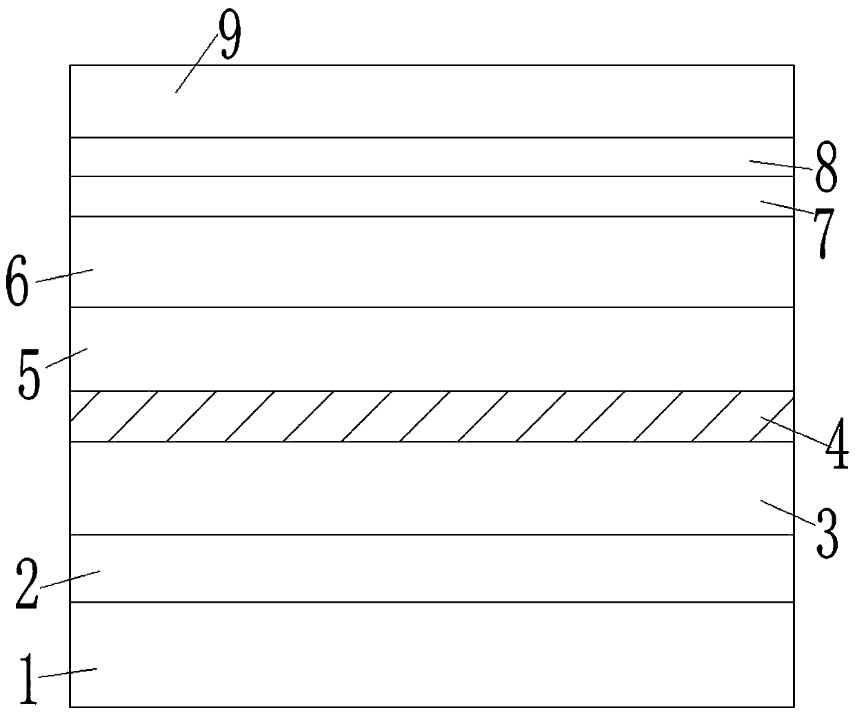
[0036] Example 1, the preferred thickness of the GaAs buffer layer 1 is 150nm, the preferred thickness of the corrosion barrier layer 2 is 400nm, the preferred thickness of the ohmic contact layer 3 is 150nm, and the preferred thickness of the N-AlxGa1-xInP first roughened layer 4 is 3um , The preferred thickness of the N-AlxGa1-xInP second roughening layer 5 is 0.45um, the preferred thickness of the lower confinement layer 6 is 500nm, the preferred thickness of the multi-quantum well light-emitting region 7 is 0.1um, and the preferred thickness of the upper confinement layer 8 is 300nm, the preferred thickness of the current spreading layer 9 is 3um.

[0037] The specific preparation method of the flip-chip LED epitaxial wafer with the above-mentioned GaAs-based roughened layer structure is as follows, which sequentially includes the following steps:

[0038] a) Place the GaAs substrate in the growth chamber of the MOCVD equipment, and pass through , heat up to 750±20°C and...

Embodiment 2

[0054] The doping concentration in step b) is 1E17-5E18 atoms / , the doping concentration in step c) is 1E17-5E18 atoms / , the doping concentration in step d) is 1E18-5E18 atoms / , the doping concentration in step e) is 1E17-1E18 atoms / , the doping concentration of AlGaAs in step f) is 1E17-5E18 atoms / , the doping concentration of AlAs is 1E17-5E18 atoms / , the doping concentration in step g) is 1E17-5E18 atoms / , the doping concentration in step h) is 1E18-5E18 atoms / , the doping concentration in step i) is 1E17-1E18 atoms / , the doping concentration in step g) is 5E18-1E20 atoms / . Preferably, the doping concentration in step b) is 2E18 atoms / , the doping concentration in step c) is 5E17 atoms / , the doping concentration in step d) is 1E18 atoms / , the doping concentration in step e) is 5E17 atoms / , the doping concentration of AlGaAs in step f) is 5E17 atoms / , the doping concentration of AlAs is 1E18 atoms / , the doping concentration in ste...

Embodiment 3

[0056] GaAs buffer layer 1, N-Al x Ga 1-x InP first roughening layer 4, N-Al x Ga 1-x The N-type dopant source of the As second roughening layer 5 and the AlInP lower confinement layer 6 is ; The P-type dopant source of confinement layer 8 and current spreading layer 9 on AlInP is .


PUM

PropertyMeasurementUnit
Thicknessaaaaaaaaaa
Thicknessaaaaaaaaaa
Thicknessaaaaaaaaaa

Abstract

The invention relates to an inverted LED epitaxial wafer of a GaAs-based armoring layer structure and a manufacturing method of the inverted LED epitaxial wafer. The inverted LED epitaxial wafer sequentially comprises a GaAs substrate, a GaAs buffer layer, a corrosion blocking layer, an ohmic contact layer, an N-Al<x>Ga<1-x>InP first armoring layer, an N-Al<x>Ga<1-x>InP second armoring layer, a lower limitation layer, a multi-quantum well luminous region, an upper limitation layer and a current extension layer from bottom to top. By arranging the second armoring layer, the inverted LED epitaxial wafer is matched with a conventional structure lattice, the high-quality armoring layer matched with the lattice can be enabled to grow in a matching way at a relatively high growth speed, the carbon-oxygen content can be prevented, the crystal growth quality is improved, the current extension and the optical characteristic are ensured, and the reliability and the stability of the device are improved; since the Al<x>Ga<1-x>As material can be grown at a high speed, the process time of an inverted LED is shortened by 20-35%, the product can be produced on a large scale, the external quantum efficiency can be greatly improved, so that the light efficiency of the product is greatly improved; and the brightness of the inverted LED can be improved by 60-80% compared with a traditional structure, and thus, the high-efficiency inverted LED can be produced on a large scale.

Description

technical field [0001] The invention relates to the field of optoelectronics, in particular to a flip-chip LED epitaxial wafer with a GaAs-based roughened layer structure and a preparation method thereof. Background technique [0002] The reason why flip chip is called "flip chip" is relative to the traditional wire bonding connection method (WireBonding) and the process after ball planting. The electrical side of the traditional chip connected to the substrate by wire bonding faces up, while the electrical side of the flip chip faces down, which is equivalent to turning the former upside down, so it is called a flip chip. [0003] In the field of chips, in order to avoid affecting the luminous efficiency due to the occupation of the light-emitting area by the electrodes in the front-mounted chip, the flip-chip technology is gradually used, especially in the application market of high-power, external lighting, and urban lighting projects. [0004] For flip-chip LED chips, a...

Claims


Application Information

Patent Timeline
IPC IPC(8): H01L33/32H01L33/22H01L33/06H01L33/14
CPCH01L33/06H01L33/14H01L33/22H01L33/32
Inventor 李志虎于军张新肖成峰
Owner Shandong Huaguang Optoelectronics Co. Ltd.
Why Eureka
Try Eureka