A three-dimensional self-limiting method for the precise fabrication of silicon nanowire pillars

A silicon nanowire, self-limiting technology, applied in nanotechnology, nanotechnology, semiconductor/solid-state device manufacturing, etc., can solve the problem of inability to achieve three-dimensional (lateral processing, etc.), and achieve the effect of high production efficiency

Active Publication Date: 2021-06-04
JIANGSU LEUVEN INSTR CO LTD
View PDF10 Cites 0 Cited by
  • Summary
  • Abstract
  • Description
  • Claims
  • Application Information

AI Technical Summary

Problems solved by technology

[0012] 2) This method cannot achieve three-dimensional (transverse processing) due to the directionality of ion removal, which will be limited in the field of three-dimensional processing such as nanowire processing in the future

Method used


Image

  • A three-dimensional self-limiting method for the precise fabrication of silicon nanowire pillars

Examples


Embodiment 1

[0038] A three-dimensional self-limiting method for precisely manufacturing silicon nanowire columns, comprising the following steps:

[0039] 1) The formation of a self-limiting oxide layer (Si-O) on the surface of Si; the formation of Si-O bonds is very easy and the thickness is very well controlled. 2 It is easy to form SiO 2 layer and has good self-limiting properties, the thickness is only 1 to several atoms thick, so the thermal reaction is very easy to achieve and has good self-limiting properties;

[0040] 2) removal of excess O atmosphere;

[0041] 3) Selective chemical etching away the SiO layer; gaseous hydrogen fluoride (Vapor HF) can etch SiO 2 , the reaction is: SiO 2 +4HF (gaseous state) = SiF 4 (gaseous)+2H 2 O (gaseous) and does not react with Si, so this step also has good self-limiting characteristics;

[0042] 4) Steps 1) to 3) are repeated to realize precise control of the etching amount.

Embodiment 2

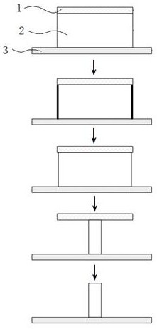
[0044] A method for precisely manufacturing silicon nanowire columns from three-dimensional self-limitation, as in Example 1, such as figure 1 As shown, wherein: the barrier layer 3 (HfO 2 ), thickness 1-10nm, silicon 2 (Si), thickness 50-100nm, hard mask layer 1 (Al 2 o 3 ), with a thickness of 1-10nm; use conventional photolithography to produce lines or columns with a size of 90nm-45nm, and remove the photoresist;

[0045] 1) Then control the substrate temperature (0-200°C) in the vacuum reaction chamber, use O 2 Treatment 1~10s, SiO 2 The thickness is about 3A; then the chamber is evacuated to leave O 2 ;

[0046] 2) Introduce HF gas, process for 1-10s, let HF convert SiO 2Selective etching away, because the fluorides of Hf and Al have very high boiling points, so under the self-passivation of their fluorides, HF will not corrode the masking layer and barrier layer. Then evacuate the residual HF and generated gas in the cavity.

[0047] 3) Repeat the above steps an...


PUM

PropertyMeasurementUnit
thicknessaaaaaaaaaa
thicknessaaaaaaaaaa

Abstract

The invention discloses a three-dimensional self-limiting method for precisely manufacturing silicon nanowire columns, which comprises the following steps: 1) forming a self-limiting oxide layer on the Si surface; 2) removing excess O atmosphere; 3) selectively chemically etching off the SiO layer ; 4) Repeat steps 1) to 3) to achieve precise control of the etching amount. The three-dimensional self-limiting and precise manufacturing method of silicon nanowire pillars of the present invention not only has the self-limiting ability at the atomic level, but also can realize three-dimensional (horizontal and vertical processing) processing, and the control ability of the device itself does not need to be as high as the existing technical solutions .

Description

technical field [0001] The invention belongs to the technical field of manufacturing semiconductor chips or nano-microstructures, and in particular relates to a three-dimensional self-limiting method for precisely manufacturing silicon nanowire columns. Background technique [0002] An integrated circuit (integrated circuit) is a tiny electronic device or component. Using a certain process, the transistors, resistors, capacitors, inductors and other components required in a circuit are interconnected, and they are fabricated on a small or several small semiconductor wafers or dielectric substrates, and then packaged in a tube. , and become a microstructure with required circuit functions; all the components in it have been structurally integrated, making electronic components a big step towards miniaturization, low power consumption, intelligence and high reliability. It is represented by the letter "IC" in the circuit. The inventors of the integrated circuit are Jack Kilb...

Claims


Application Information

Patent Timeline
Patent Type & Authority Patents(China)
IPC IPC(8): H01L21/306B82Y30/00B82Y40/00
CPCB82Y30/00B82Y40/00H01L21/30608
Inventor 许开东
Owner JIANGSU LEUVEN INSTR CO LTD
Why Eureka
Try Eureka