LED light transmitter
A technology for optical transmitters and LED chips, applied in electromagnetic transmitters, optical fiber transmission, electrical components, etc., can solve problems such as low luminous efficiency and low output power of LED optical transmitters, and achieve high luminous efficiency, low cost, and improved The effect of transmission performance
- Summary
- Abstract
- Description
- Claims
- Application Information
AI Technical Summary
Problems solved by technology
Method used
Image
Examples
Embodiment 1
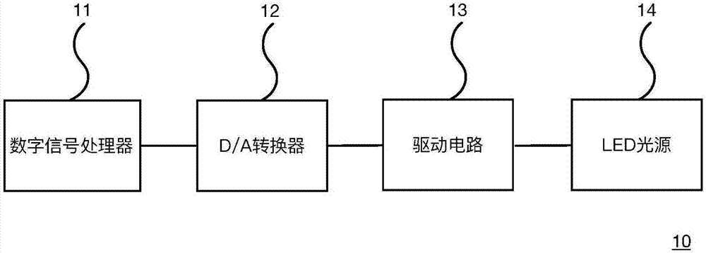
[0042] See figure 1 , figure 1 A schematic structural diagram of an LED light transmitter provided in an embodiment of the present invention; the LED light transmitter 10 includes:
[0043] digital signal processor 11;
[0044] D / A converter 12, is electrically connected with described digital signal processor 11;
[0045] A drive circuit 13 electrically connected to the D / A converter 12;
[0046] LED light source 14, is electrically connected with described driving circuit 13, and comprises LED light-emitting diode 20;
[0047] Preferably, the digital signal processor 11 adopts a programmable gate array FPGA.
[0048] Preferably, the LED light transmitter 10 also includes an automatic power control circuit.
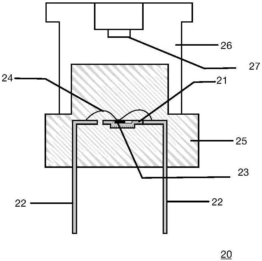
[0049] See figure 2 , figure 2 A schematic structural view of an LED light-emitting diode provided in an embodiment of the present invention;
[0050] Further, the LED light emitting diode 20 includes:
[0051] Carrier 21;
[0052] pin 22;
[0053] chip base...
Embodiment 2
[0082] Please refer to Figure 4a-Figure 4j , Figure 4a-Figure 4j A schematic diagram of the preparation process of a vertical PiN light-emitting diode according to an embodiment of the present invention. The preparation method includes the following steps:
[0083] S101, select the doping concentration as 5×10 18 cm -3 P-type monocrystalline silicon (Si) substrate sheet 001, such as Figure 4a shown.
[0084] S102. At a temperature of 275° C. to 325° C., a Ge seed layer 002 of 40 to 50 nm is grown on the surface of the Si substrate by a CVD process, such as Figure 4b shown.
[0085] S103. At a temperature of 500° C. to 600° C., a Ge main layer 003 of 150 to 250 nm is grown on the surface of the Ge seed crystal layer by using a CVD process, such as Figure 4c shown.
[0086] S104, using CVD process to grow 100-150nm SiO on the surface of Ge main body layer 2 Oxide layer 004, such as Figure 4d shown.
[0087] S105. Heat the entire substrate material including the s...
PUM
| Property | Measurement | Unit |
|---|---|---|
| Luminous wavelength | aaaaa | aaaaa |
| Thickness | aaaaa | aaaaa |
Abstract
Description
Claims
Application Information


