
Pattern Sapphire Substrate, and mask and method for manufacturing Pattern Sapphire Substrate

A technology for sapphire substrates and graphic substrates, which is applied to the photolithographic process of patterned surfaces, originals for photomechanical processing, semiconductor/solid-state device manufacturing, etc., which can solve reverse leakage, affect device extraction efficiency, reduce LED internal quantum efficiency and reliability issues, to achieve the effect of suppressing defect extension, releasing adaptation stress, and reducing dislocation density

Inactive Publication Date: 2017-11-10
SHANGHAI MICRO ELECTRONICS EQUIP (GRP) CO LTD
View PDF3 Cites 1 Cited by
  • Summary
  • Abstract
  • Description
  • Claims
  • Application Information

AI Technical Summary

Problems solved by technology

As for the external quantum efficiency, assuming that the refractive index of air is 1, since the refractive index of sapphire (about 1.67) and the refractive index of GaN material (about 2.45) are both greater than the refractive index of air, the photons generated in the active region of the substrate occur multiple times Total reflection, which seriously affects the light extraction efficiency of the device
At the same time, there is a large lattice mismatch (about 16%) and thermal expansion absorption mismatch (34%) between the sapphire substrate and the GaN material, which will cause a large number of defects in the growth process of GaN, causing reverse leakage and other defects. impact, reducing the internal quantum efficiency and reliability of the LED

Method used


Image

  • Pattern Sapphire Substrate, and mask and method for manufacturing Pattern Sapphire Substrate
  • Pattern Sapphire Substrate, and mask and method for manufacturing Pattern Sapphire Substrate
  • Pattern Sapphire Substrate, and mask and method for manufacturing Pattern Sapphire Substrate

Examples


Embodiment 1

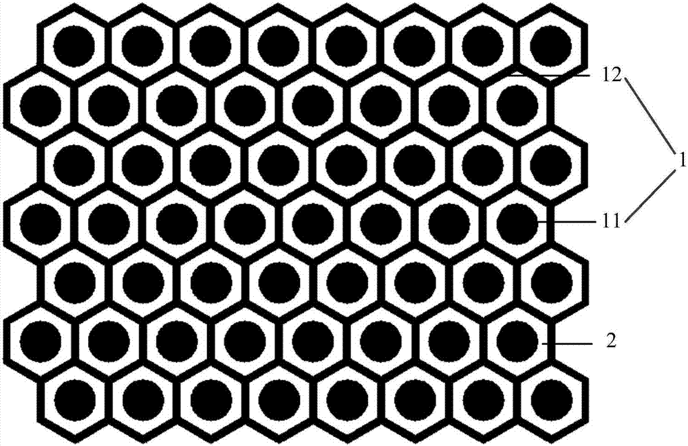
[0043] Please refer to figure 1 , the present invention provides a mask for making a sapphire substrate, which consists of a non-transparent region 1 and a translucent region 2. In the figure, the non-transmissive region 1 is composed of periodically arranged circular non-transparent regions 11 and periodic Arranged regular hexagons, the regular hexagons are formed by the end-to-end connection of non-transparent lines 12, adjacent regular hexagons share one side, and the circular non-transparent area 11 is located inside the regular hexagon, except for the above-mentioned circular non-transparent The area 11 and the non-light-transmitting lines 12, and the rest are the light-transmitting areas 2.

[0044] Preferably, the diameter of the circular non-transparent regions 11 is 1.6 μm, and the distance between the centers of adjacent circular non-transparent regions 11, that is, the period of the circular non-transparent regions 11 is 15 μm, which is not The width of the light-t...

Embodiment 2

[0060] The difference between this embodiment and Embodiment 1 is that the mask used is as Figure 4 As shown, the mask is also composed of a light-transmitting area 2 and a non-transmitting area 1, wherein the light-transmitting area 2 is a circular ring-shaped light-transmitting area 21 arranged periodically, and the circular non-transparent area 11 is located in the ring-shaped transparent area. Inside Light Zone 21.

[0061] Preferably, the radius of the circular non-transparent region 11 on the above-mentioned mask is 0.8 μm, and the width of the annular light-transmissive region 21 is 0.7 μm. Using this mask to prepare a sapphire pattern substrate, the following is obtained: Figure 4 structure shown.

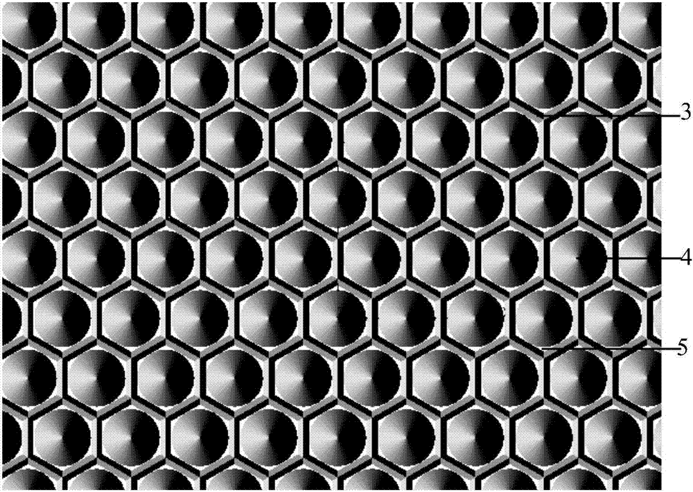
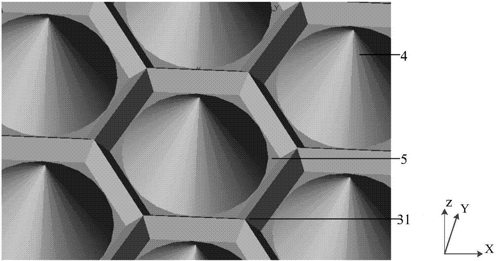
[0062] Please refer to Figure 5 with Image 6 , a cone 4 is formed on the sapphire pattern substrate, and a hexagonal partition wall 3 is formed around each cone 4, and the bottom of each hexagonal partition wall 3 and the bottom surface of the cone 4 are located on t...


PUM

PropertyMeasurementUnit
Base radiusaaaaaaaaaa
Radiusaaaaaaaaaa
Widthaaaaaaaaaa

Abstract

In the sapphire pattern substrate provided by the present invention and the mask plate and manufacturing method for making the sapphire pattern substrate, a closed partition wall is set up outside the periodically arranged structural patterns on the substrate, and every two adjacent structural patterns Compared with the sapphire pattern substrate without a wall in the prior art, the present invention has more reflective surfaces, which is used to provide a larger area for epitaxial growth, which is beneficial to reduce the The dislocation density makes it possible to better release the adaptive stress generated inside the crystal due to the previous manufacturing process, thereby reducing the defect density and improving the luminous efficiency of the LED chip.

Description

technical field [0001] The invention relates to the field of semiconductor photolithography, in particular to a sapphire pattern substrate, a mask and a method for making the sapphire pattern substrate. Background technique [0002] LED chips, also known as LED light-emitting chips, are the core components of LED lights, which refers to the P-N junction. Its main function is to convert electrical energy into light energy. The main material of the LED chip is monocrystalline silicon. LED chip is made up of two parts, and a part is P-type semiconductor, and hole is dominant in its structure, and the other end is N-type semiconductor, and what occupy the leading position inside is electron. Time these two kinds of semiconductors couple together, between them, just form a P-N junction. When electric current acts on this chip by wire time, electron will be pushed to P district, and in P district, electron is with hole recombination, then will send energy with the form of photon...

Claims


Application Information

Patent Timeline
IPC IPC(8): H01L33/20H01L33/22G03F1/00H01L21/027H01L21/3065
CPCH01L33/20G03F1/00H01L21/0274H01L21/3065H01L33/22
Inventor 晏小平李成立顾威威王武
Owner SHANGHAI MICRO ELECTRONICS EQUIP (GRP) CO LTD
Learn More