Preparation method of trench type Schottky diode

A Schottky diode and trench type technology, which is applied in semiconductor/solid-state device manufacturing, electrical components, circuits, etc., can solve poor contact, low Schottky barrier, and affect the performance of trench Schottky diodes and other problems, to achieve the effect of good contact, good Schottky barrier, and improved performance

Inactive Publication Date: 2017-11-14
PEKING UNIV FOUNDER GRP CO LTD +1
View PDF3 Cites 3 Cited by
  • Summary
  • Abstract
  • Description
  • Claims
  • Application Information

AI Technical Summary

Problems solved by technology

[0005] The invention provides a method for preparing a trench-type Schottky diode, which is used to solve the problem of forming between the N-type epitaxial layer and the metal layer between adjacent silicon trenches of the trench-type Schottky diode obtained in the prior art. The Schottky barrier is not in good contact, and the Schottky barrier is not high, resulting in a very large reverse leakage, which in turn affects the performance of the trench Schottky diode.

Method used


Image

  • Preparation method of trench type Schottky diode
  • Preparation method of trench type Schottky diode
  • Preparation method of trench type Schottky diode

Examples


Embodiment Construction

[0044] In order to make the purpose, technical solutions and advantages of the embodiments of the present invention clearer, the technical solutions in the embodiments of the present invention will be clearly and completely described below in conjunction with the drawings in the embodiments of the present invention. Obviously, the described embodiments It is a part of embodiments of the present invention, but not all embodiments. Based on the embodiments of the present invention, all other embodiments obtained by persons of ordinary skill in the art without making creative efforts belong to the protection scope of the present invention.

[0045] figure 1 The schematic flow chart of the preparation method of the trench-type Schottky diode provided in Embodiment 1 of the present invention, in order to clearly and systematically describe the method in this embodiment, as figure 1 shown, including:

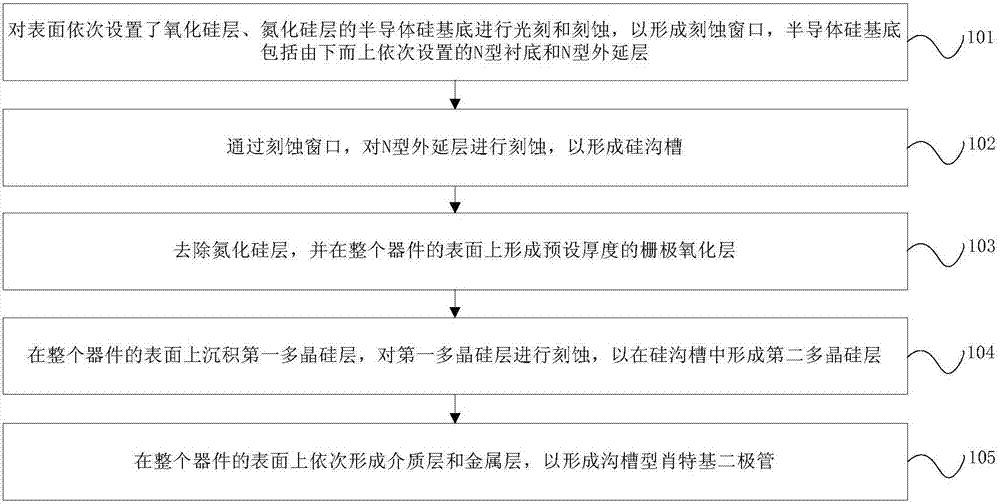
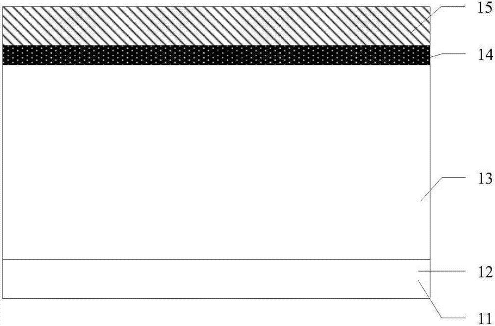
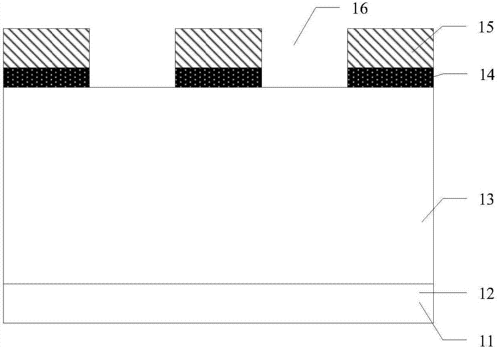
[0046] Step 101: Perform photolithography and etching on the semiconductor sili...


PUM

PropertyMeasurementUnit
thicknessaaaaaaaaaa
thicknessaaaaaaaaaa
thicknessaaaaaaaaaa

Abstract

The present invention provides a preparation method of a trench type Schottky diode. The method includes the following steps that: photoetching and etching are performed on a semiconductor silicon substrate of which the surface is sequentially provided with a silicon oxide layer and a silicon nitride layer, so that etching windows can be formed; by means of the etching windows, the N type epitaxial layer of the semiconductor silicon substrate is etched, so that silicon trenches can be formed; the silicon nitride layer is removed, so that a gate oxide layer can be formed on the surface of the entire device; a first polycrystalline silicon layer is deposited on the surface of the entire device, the first polycrystalline silicon layer is etched, so that a second polycrystalline layer is formed in the silicon trenches; and a dielectric layer and a metal layer are sequentially formed on the surface of the entire device. The N type epitaxial layer among adjacent silicon trenches can well contact with the metal layer, so that the contact performance of a Schottky barrier formed between the N type epitaxial layer among the adjacent silicon trenches and the metal layer can be excellent; and since the Schottky barrier is good, the reverse current leakage of the trench type Schottky diode can be decreased, and the performance of the trench type Schottky diode can be improved.

Description

technical field [0001] The invention relates to the field of semiconductor technology, in particular to a method for preparing a trench Schottky diode. Background technique [0002] As a key component of the circuit system, power diodes are widely used in civilian products such as high-frequency inverters, digital products, generators, and televisions, as well as in military equipment such as satellite receivers, missiles, and aircraft. . At present, the commonly used types of power diodes include ordinary rectifier diodes and Schottky diodes. Among them, due to the characteristics of low on-state voltage drop, low leakage current, and small reverse recovery time of Schottky diodes, they are widely used in various equipment; and the grooves in Schottky diodes Trench-type Schottky diodes have low forward voltage drop and high die area utilization, so trench-type Schottky diodes are attracting more and more attention. [0003] In the prior art, the preparation method of the...

Claims


Application Information

Patent Timeline
Patent Type & Authority Applications(China)
IPC IPC(8): H01L21/329H01L29/06
CPCH01L29/66143H01L29/0657
Inventor 赵圣哲李理赵文魁
Owner PEKING UNIV FOUNDER GRP CO LTD
Why Eureka
Try Eureka