Driving control circuit for multiple SiC MOSFET chip parallel power module and printed circuit board thereof

A technology for driving control circuits and printed circuit boards, applied in the field of power electronics, can solve problems such as fast switching speed of SiC MOSFETs, and achieve the effects of reducing inductance, improving current sharing, and reducing reliability

Active Publication Date: 2017-11-21
XI AN JIAOTONG UNIV
View PDF3 Cites 2 Cited by
  • Summary
  • Abstract
  • Description
  • Claims
  • Application Information

AI Technical Summary

Problems solved by technology

However, the switching speed of SiC MOSFET is fast, which puts forward higher requirements for driving layout and current sharing of parallel chips. Therefore, it is necessary to develop a technology that can realize the driving of power modules connected in parallel with multiple SiC MOSFET chips, and at the same time ensure the safe and stable operation of each SiC MOSFET chip.

Method used


Image

  • Driving control circuit for multiple SiC MOSFET chip parallel power module and printed circuit board thereof
  • Driving control circuit for multiple SiC MOSFET chip parallel power module and printed circuit board thereof
  • Driving control circuit for multiple SiC MOSFET chip parallel power module and printed circuit board thereof

Examples


Embodiment Construction

[0020] The present invention is described in further detail below in conjunction with accompanying drawing:

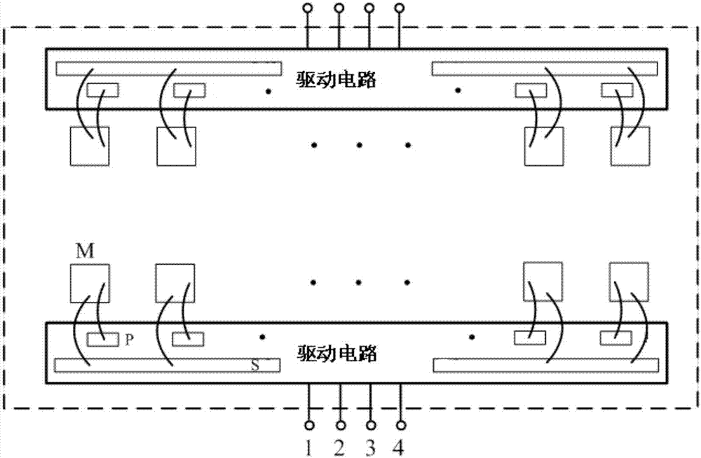
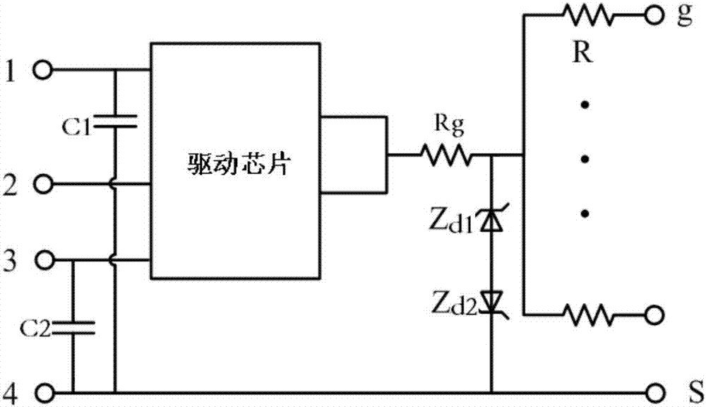
[0021] refer to figure 1 and figure 2 , the multi-SiC MOSFET chip parallel power module drive control circuit according to the present invention includes a positive voltage input terminal 1, a negative voltage input terminal 3, a drive signal input terminal 2, a ground wire 4, a drive chip, a first decoupling capacitor C1, a second Two decoupling capacitors C2, total drive resistor Rg, first zener diode Zd1, second zener diode Zd2, N drive current sharing resistors R and N control terminals g, where one drive current sharing resistor R corresponds to one SiC MOSFET chip and a control terminal g; wherein, the positive voltage input terminal 1 is connected with one end of the first decoupling capacitor C1 and the driver chip, and the negative voltage input terminal 3 is connected with one end of the second decoupling capacitor C2 and the driver chip, The drive signal ...


PUM


Abstract

The invention discloses a driving control circuit for a multiple SiC MOSFET chip parallel power module and a printed circuit board thereof. The driving control circuit comprises a positive voltage input terminal, a negative voltage input terminal, a driving signal input terminal, a ground wire, a driving chip, a first decoupling capacitor, a second decoupling capacitor, a total driving resistor, a first voltage stabilizing diode, a second voltage stabilizing diode, N driving current-sharing resistors and N control terminals. The circuit and the printed circuit board thereof can implement driving on the multiple SiC MOSFET chip parallel power module and meanwhile, ensure safe and stable operation of each SiC MOSFET chip.

Description

technical field [0001] The invention belongs to the technical field of power electronics, and in particular relates to a driving control circuit of a multi-SiC MOSFET chip parallel power module and a printed circuit board thereof. Background technique [0002] With the development of power electronic technology, the power level of power electronic devices is getting higher and higher. In order to meet the requirements of power electronic devices, the current level of power semiconductors also needs to be further improved. At this stage, the current level of a single power semiconductor chip is far from meeting the demand for semiconductor switches in modern power electronic devices, and multiple semiconductor chips need to be used in parallel. [0003] In the parallel application of power semiconductor chips, the asynchrony of the driving signal and the asymmetry of the chip layout will cause overcurrent and overheating damage to the semiconductor chip, which will affect th...

Claims


Application Information

Patent Timeline
Patent Type & Authority Applications(China)
IPC IPC(8): H02M1/088
CPCH02M1/088Y02B70/10
Inventor 任宇杨旭张帆乔梁
Owner XI AN JIAOTONG UNIV
Why Eureka
Try Eureka