Composite electrode and preparation method thereof, and heterojunction solar cell and preparation method thereof

A technology of solar cells and composite electrodes, applied in circuits, photovoltaic power generation, electrical components, etc., can solve the problem that the photoelectric conversion efficiency needs to be further improved.

Inactive Publication Date: 2017-11-24
GCL SYST INTEGRATION TECH +1
View PDF7 Cites 5 Cited by
  • Summary
  • Abstract
  • Description
  • Claims
  • Application Information

AI Technical Summary

Problems solved by technology

[0005] Based on this, it is necessary to provide a new composite electrode structure fo

Method used


Image

  • Composite electrode and preparation method thereof, and heterojunction solar cell and preparation method thereof
  • Composite electrode and preparation method thereof, and heterojunction solar cell and preparation method thereof
  • Composite electrode and preparation method thereof, and heterojunction solar cell and preparation method thereof

Examples


preparation example Construction

[0076] A method for preparing a compound electrode structure of a heterojunction solar cell, comprising the steps of:

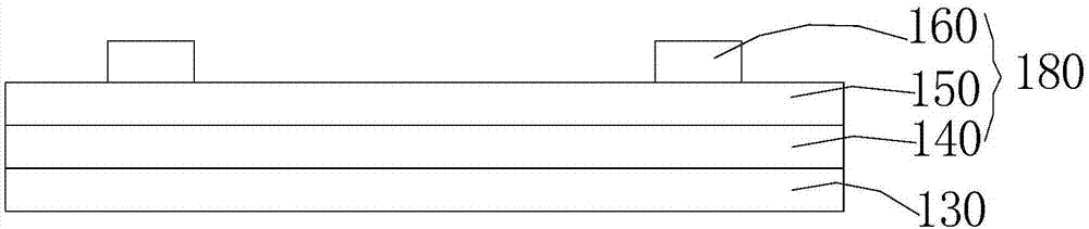
[0077] An interface buffer layer is formed on the doped amorphous silicon layer; when the doped amorphous silicon layer is P-type, the work function of the interface buffer layer is greater than or equal to 5V; when the doped amorphous silicon layer is N-type, the interface buffer layer The work function is less than or equal to 4.2eV;

[0078] forming a transparent conductive layer on the interface buffer layer;

[0079] Electrodes are formed on the transparent conductive layer.

[0080] Preferably, when the doped amorphous silicon layer is P-type, the interface buffer layer is formed by physical vapor deposition. For example, vacuum evaporation or sputter evaporation formation.

[0081] Preferably, when the interface buffer layer is lithium fluoride or cesium fluoride, the interface buffer layer is deposited by vacuum evaporation. When the interface buf...

Embodiment 1

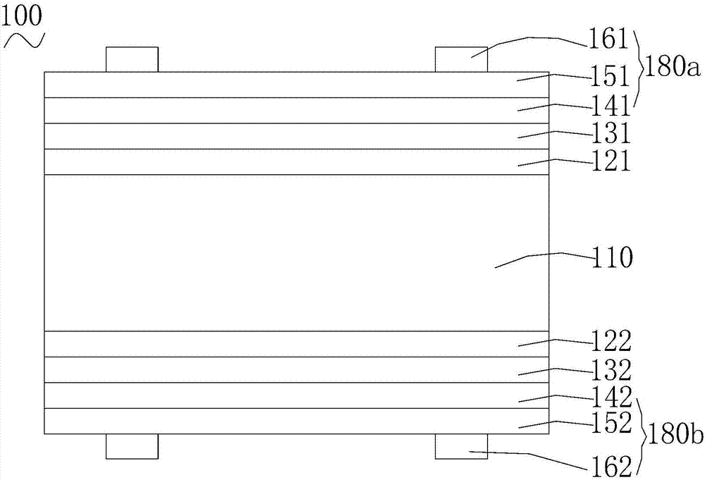
[0090] The N-type crystalline silicon wafer is passed through an alkaline solution to remove the damaged layer; the N-type crystalline silicon wafer is cleaned and textured, and the surface phosphosilicate glass is removed.

[0091] On one surface of the N-type crystalline silicon wafer, the intrinsic hydrogenated amorphous silicon film (i-a-Si:H) and the N-type hydrogenated amorphous silicon film (n-a-Si:H) are deposited by PECVD to form the second intrinsic layer and a second doped amorphous silicon layer.

[0092] On the other surface of the N-type crystalline silicon wafer, the intrinsic hydrogenated amorphous silicon film (i-a-Si:H) and the P-type hydrogenated amorphous silicon film (p-a-Si:H) were deposited by PECVD to form the first intrinsic layer and the first doped amorphous silicon layer.

[0093] Non-stoichiometric molybdenum oxide is grown on the first doped amorphous silicon layer by vacuum evaporation with a thickness of 6 nm.

[0094] Reactive plasma depositi...

Embodiment 2

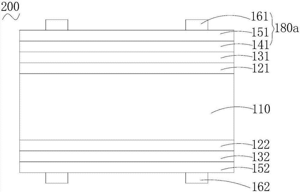
[0098] The N-type crystalline silicon wafer is passed through an alkaline solution to remove the damaged layer; the N-type crystalline silicon wafer is cleaned and textured, and the surface phosphosilicate glass is removed.

[0099] On one surface of the N-type crystalline silicon wafer, the intrinsic hydrogenated amorphous silicon film (i-a-Si:H) and the N-type hydrogenated amorphous silicon film (n-a-Si:H) are deposited by PECVD to form the second intrinsic layer and a second doped amorphous silicon layer.

[0100] On the other surface of the N-type crystalline silicon wafer, the intrinsic hydrogenated amorphous silicon film (i-a-Si:H) and the P-type hydrogenated amorphous silicon film (p-a-Si:H) were deposited by PECVD to form the first intrinsic layer and the first doped amorphous silicon layer.

[0101] Non-stoichiometric molybdenum oxide is grown on the first doped amorphous silicon layer by vacuum evaporation with a thickness of 6 nm.

[0102] Non-stoichiometric titan...


PUM

PropertyMeasurementUnit
Work functionaaaaaaaaaa
Thicknessaaaaaaaaaa

Abstract

The present invention relates to the composite electrode structure of a heterojunction solar cell comprising a transparent conductive layer, an electrode arranged on the transparent conductive layer and an interface buffer layer configured to reduce the interface resistance between the transparent conductive layer and a doped noncrystalline silicon layer; when the electrode is a positive pole, the work function of the interface buffer layer is larger than or equal to 5V; and when the electrode is a negative pole, the work function of the interface buffer layer is smaller than or equal to 4.2eV. In the composite electrode structure of the heterojunction solar cell, the interface buffer layer is inserted between the doped noncrystalline silicon layer and the transparent conductive layer to reduce the interface resistance between the doped noncrystalline silicon layer and the transparent conductive layer so as to improve the filling factors of the battery, match the energy grade of the battery, and finally improve the photoelectric conversion efficiency of the heterojunction solar cell. The present invention further provides a preparation method of the composite electrode structure of the heterojunction solar cell and the heterojunction solar cell and the preparation method thereof.

Description

technical field [0001] The invention relates to the field of photovoltaic technology, in particular to a composite electrode and a preparation method thereof, a heterojunction solar cell and a preparation method thereof. Background technique [0002] Heterojunction solar cells are typical high-efficiency solar cells, which have the characteristics of low temperature coefficient, no light-induced degradation (LID), no potential-induced degradation (PID), and double-sided power generation. The actual power generation of solar cells can be 15% to 30% higher than that of polysilicon cells with the same nominal power, which is especially suitable for applications in the distributed power generation market. [0003] A traditional heterojunction solar cell generally consists of a crystalline silicon wafer, a doped amorphous silicon layer, an intrinsic layer located between the crystalline silicon wafer and the doped amorphous silicon layer, and first and second electrodes. [0004...

Claims


Application Information

Patent Timeline
IPC IPC(8): H01L31/0216H01L31/0224H01L31/075H01L31/18
CPCH01L31/02167H01L31/022425H01L31/022475H01L31/075H01L31/1804H01L31/1884Y02E10/547Y02E10/548Y02P70/50
Inventor 杨黎飞张闻斌李杏兵
Owner GCL SYST INTEGRATION TECH
Why Eureka
Try Eureka