Back illuminated cascade multiplication avalanche photodiode

A technology of cascade multiplication and avalanche photoelectricity, which is applied in the direction of circuits, electrical components, semiconductor devices, etc., can solve the problems that the cascade structure is not suitable for the back-illuminated type, and cannot reach the absorption layer to form effective multiplication, so as to improve the linear multiplication ability, The effect of improved absorption and utilization capacity and high electron ionization rate

Active Publication Date: 2017-11-28
INST OF ELECTRONICS ENG CHINA ACAD OF ENG PHYSICS
View PDF14 Cites 8 Cited by
  • Summary
  • Abstract
  • Description
  • Claims
  • Application Information

AI Technical Summary

Problems solved by technology

However, under the back-illuminated hole injection, due to the energy band structure of the multiplication region, the ratio k of the ionization coefficient of holes and electrons is only 0.05, and the holes are basically unable to achieve collision ionization in the cascade structure to produce a multiplication effect.
At the same time, the back-incident light will be absorbed when passing through the multiplication area, and cannot reach the absorption layer to form an effective multiplication
Based on the above two points, it is proved that the existing cascade structure is not suitable for back-illuminated

Method used


Image

  • Back illuminated cascade multiplication avalanche photodiode
  • Back illuminated cascade multiplication avalanche photodiode
  • Back illuminated cascade multiplication avalanche photodiode

Examples


Embodiment 1

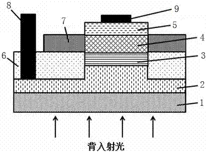
[0024] The back-illuminated cascaded multiplied avalanche photodiode for the ultraviolet band specifically refers to a back-illuminated cascaded multiplied avalanche photodiode with a dielectric light coupling and convergence structure for a detection wavelength of 350nm. The structure is followed by substrate and buffer layer 1, n-type doped Al x Ga 1-x N layer 2 , i-type periodic cascade multiplication layer 3 , i-type intrinsic absorption layer 4 and p-type electrode layer 5 . An optical coupling and converging structure layer is prepared outside the 4 mesas of the i-type intrinsic absorption layer.

[0025] Such as figure 2 As shown, in this embodiment, an AlN template buffer layer is grown on a sapphire substrate, and n-type doped Al is grown on it. x Ga1-x N layer 2, composition x=0.2, thickness 200nm, to ensure n-doped Al x Ga 1-x N layer 2 absorbs less than 10% for the 350nm detection wavelength, and the doping concentration is 1×10 18 cm -3 . The material of ...

Embodiment 2

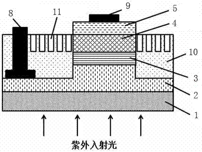
[0028] The back-illuminated cascaded multiplied avalanche photodiode for the visible band specifically refers to a back-illuminated cascaded multiplied avalanche photodiode with two dielectric optical coupling and convergence structures for a detection wavelength of 500nm. The structure is followed by substrate and buffer layer 1, n-type doped Al x Ga 1-x N layer 2 , i-type periodic cascade multiplication layer 3 , i-type intrinsic absorption layer 4 and p-type electrode layer 5 . An optical coupling and converging structure layer is prepared outside the 4 mesas of the i-type intrinsic absorption layer.

[0029] Such as image 3 As shown, in this embodiment, an AlN template buffer layer is grown on a sapphire substrate, and n-type doped Al is grown on it. x Ga 1-x N layer 2, composition x=0, thickness 1000nm, can ensure n-doped Al x Ga 1-x N layer 2 absorbs less than 5% for the detection wavelength of 500nm, and the doping concentration is 1×10 18 cm -3 . The material...

Embodiment 3

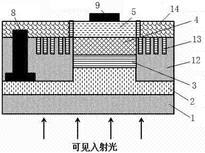
[0032] The back-illuminated cascaded multiplied avalanche photodiode for the near-infrared band specifically refers to a back-illuminated cascaded multiplied avalanche photodiode with a metal grating optical coupling convergence structure for the 1550 nm communication band. The structure is followed by substrate and buffer layer 1, n-type doped Al x Ga 1-x N layer 2 , i-type periodic cascade multiplication layer 3 , i-type intrinsic absorption layer 4 and p-type electrode layer 5 . An optical coupling and converging structure layer is prepared outside the 4 mesas of the i-type intrinsic absorption layer.

[0033] Such as Figure 4 As shown, in this embodiment, an AlN template buffer layer is grown on a sapphire substrate, and n-type doped Al is grown on it. x Ga 1-x N layer 2, composition x=0, thickness 1000nm, can ensure n-doped Al x Ga 1-x N layer 2 absorbs less than 5% for the detection wavelength of 1550nm, and the doping concentration is 1×10 18 cm -3 . The mater...


PUM


Abstract

The invention discloses a back illuminated cascade multiplication avalanche photodiode. A buffering layer, an n-type AlxGa1-xN layer, an i-type periodical cascade multiplication layer, an i-type intrinsic absorbing layer and a p-type electrode layer are successively arranged from bottom to top on a substrate. An optical coupling gathering structure is arranged at the periphery of the i-type intrinsic absorbing layer tabletop. According to the back illuminated cascade multiplication avalanche photodiode, through the optical coupling gathering structure, a problem of low effective absorption rate of a periodical cascade multiplication structure in back illumination is effectively settled, and furthermore dimension of a device tabletop is reduced and body leakage current is reduced. According to the back illuminated cascade multiplication avalanche photodiode, a solution for effective operation of a periodical cascade multiplication avalanche photodiode in back illumination is generated. The back illuminated cascade multiplication avalanche photodiode is suitable for large-scale array integration and is suitable for multiple wavebands in ultraviolet light, visible light and near-infrared light, and furthermore can be widely used in weak light detection imaging and single-photon detection imaging.

Description

technical field [0001] The invention relates to the field of photoelectric detection and single photon detection, in particular to a back-illuminated cascaded multiplied avalanche photodiode. Background technique [0002] High-sensitivity, low-noise weak light detection has great application value in the fields of secure communication, early warning and guidance, fire early warning, atmospheric environment monitoring, biological detection, deep space detection, etc., and is one of the main directions for the development of photoelectric detection technology. Common high-sensitivity ultraviolet-visible-near-infrared detectors for weak light detection mainly include photomultiplier tubes (PMTs) and semiconductor avalanche detectors (APDs). Compared with PMT, APD has high quantum efficiency, low operating voltage, high reliability, and is easy to fabricate a large-scale high-resolution detector array. Although the most mature Si-based avalanche detector has good performance in...

Claims


Application Information

Patent Timeline
Patent Type & Authority Applications(China)
IPC IPC(8): H01L31/0232H01L31/0352H01L31/107
CPCH01L31/02327H01L31/03529H01L31/1075Y02P70/50
Inventor 李倩李沫陈飞良康健彬王旺平黄锋张晖张健
Owner INST OF ELECTRONICS ENG CHINA ACAD OF ENG PHYSICS
Why Eureka
Try Eureka