

Method for manufacturing semiconductor epitaxial wafer and method for manufacturing solid-state imaging device
A manufacturing method, epitaxial wafer technology, applied in semiconductor/solid-state device manufacturing, semiconductor devices, electric solid-state devices, etc., can solve insufficient problems and achieve the effect of high gettering capacity
- Summary
- Abstract
- Description
- Claims
- Application Information
AI Technical Summary
Problems solved by technology
Method used
Image

Examples
Embodiment
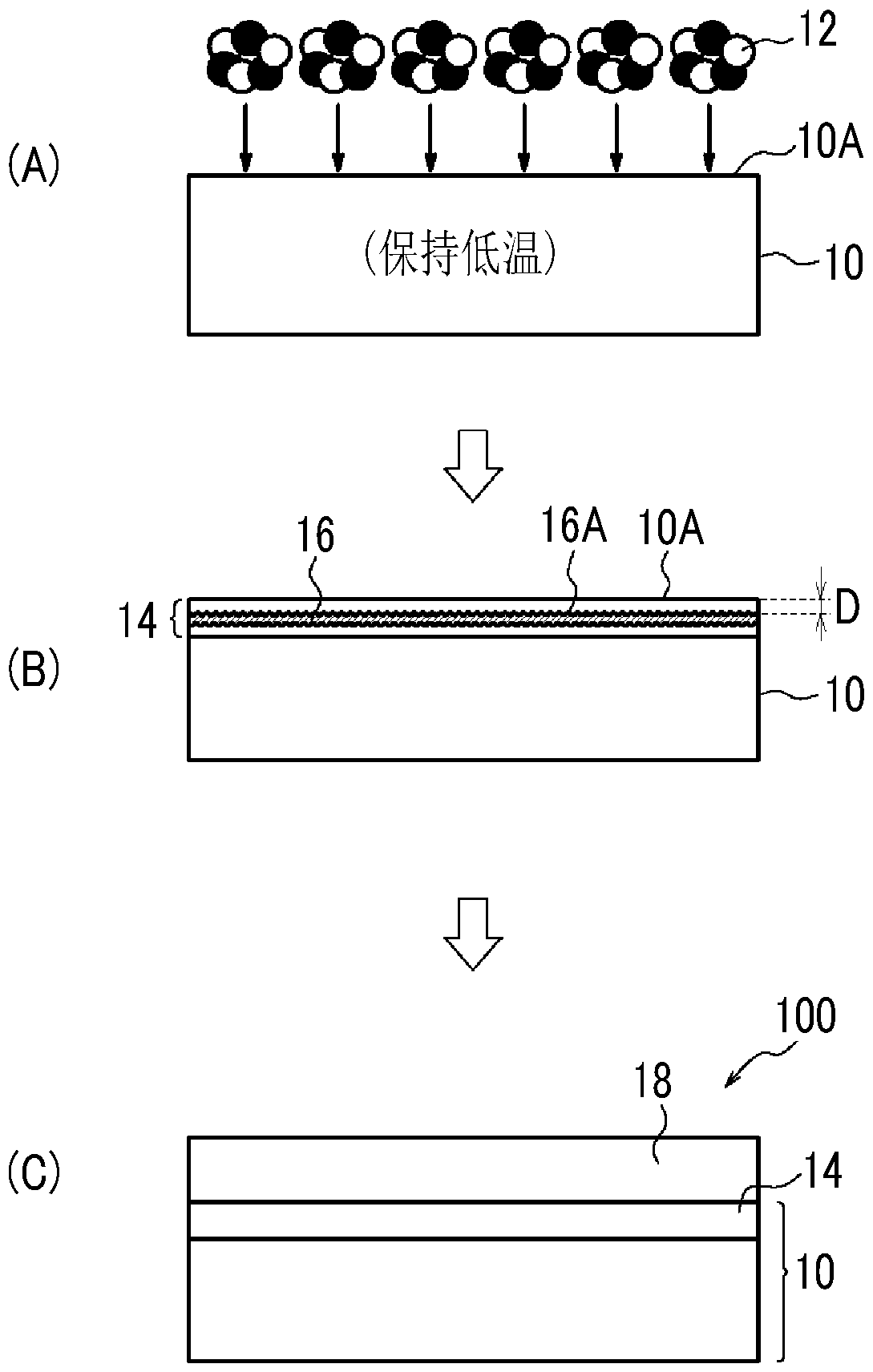
[0072] An n-type silicon wafer (diameter: 300 mm, thickness: 725 μm, dopant: phosphorus, dopant concentration: 5.0×10 14 atom / cm 3 ). Next, the C 3 h 5 Clusters are irradiated onto the surface of the silicon wafer to form a modified layer. The substrate temperature and the dose of carbon at this time were the conditions described in Table 1. The acceleration voltage per carbon atom is 23.4keV / atom, the beam current value is 800μA, the tilt (Tilt): 0°, and the twist (Twist): 0°.
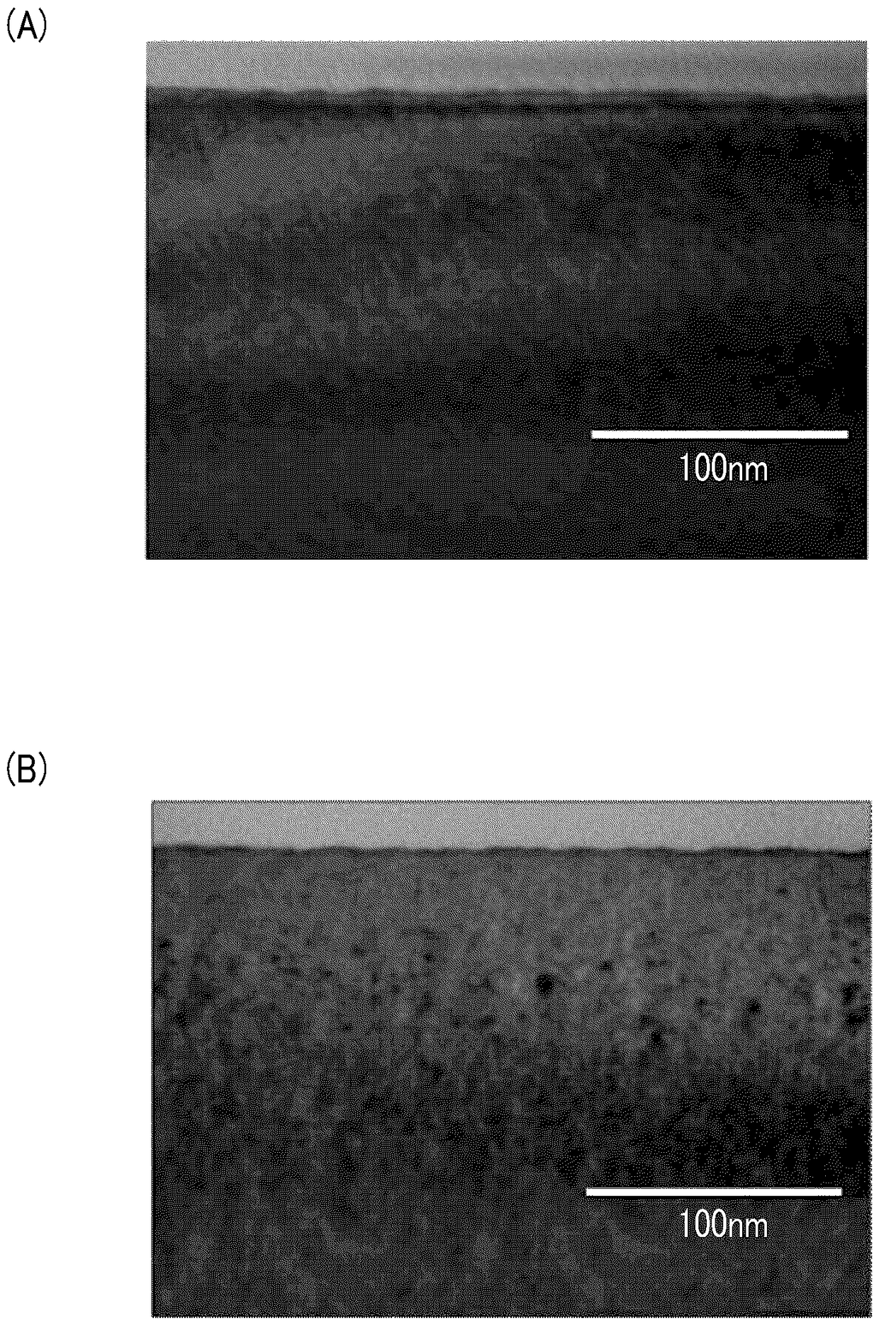
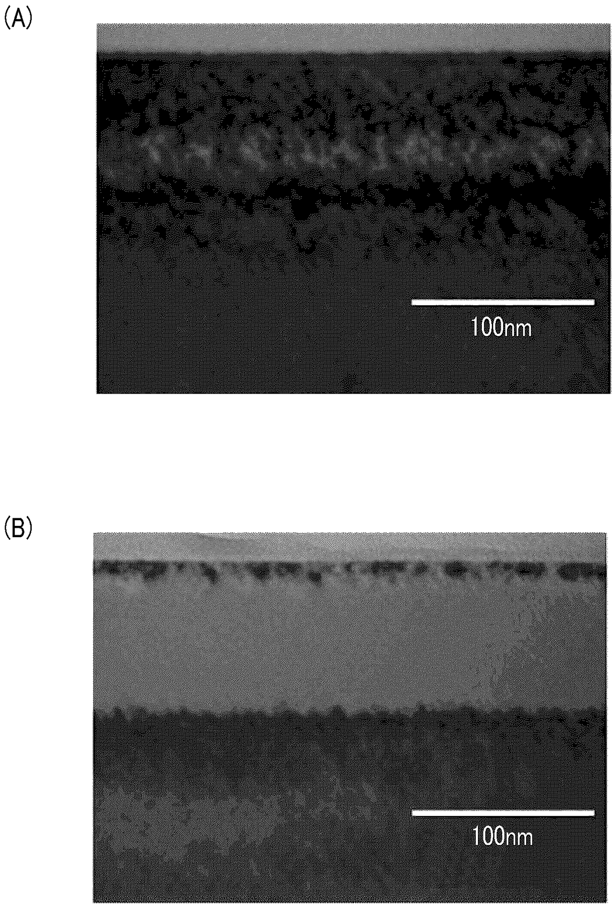
[0073] The cross section around the modified layer immediately after cluster ion irradiation was observed by TEM. Table 1 shows the presence or absence of the amorphous layer, the average depth of the surface, and the thickness in each experimental example. As a representative, No.5 in Table 1 is expressed in figure 2 In (A), No.7 is shown in figure 2 (B). In addition, No. 13 and No. 14 are shown in image 3 (A), image 3 (B). In the figure, the whitish portion is seen to be an amorphous...
PUM
 Abstract
Description
Claims
Application Information