
Connection material for connecting silicon carbide ceramics, and method for connecting silicon carbide ceramics

A technology of silicon carbide ceramics and connecting materials, which is applied in the field of connecting silicon carbide ceramics by using the connecting materials, which can solve the problems of high cost and difficulty in industrial production

Active Publication Date: 2017-12-19
NINGBO INST OF MATERIALS TECH & ENG CHINESE ACADEMY OF SCI
View PDF1 Cites 6 Cited by
  • Summary
  • Abstract
  • Description
  • Claims
  • Application Information

AI Technical Summary

Problems solved by technology

However, in order to realize the connection between silicon carbide materials, an external heat source is required to provide sufficient heat, so the cost is high and industrial production is difficult.

Method used


Image

  • Connection material for connecting silicon carbide ceramics, and method for connecting silicon carbide ceramics
  • Connection material for connecting silicon carbide ceramics, and method for connecting silicon carbide ceramics
  • Connection material for connecting silicon carbide ceramics, and method for connecting silicon carbide ceramics

Examples


Embodiment 1

[0026] In this example, if figure 1 The silicon carbide ceramic materials to be joined are shown as being joined using the joining layer material. The material to be connected is two pieces of silicon carbide with a diameter of Ф20*20mm, and the material of the connection layer is pure titanium. The silicon carbide materials to be connected are connected together through the connection layer by heating and connecting with an external heat source. The method of external heat source heating connection is electric field assisted thermocompression connection. Specific steps are as follows:

[0027] (1) Polish the silicon carbide surface to be connected with 0.1 micron diamond polishing liquid to remove larger defects and impurities on the surface;

[0028] (2) Coating a 500nm Ti film on the surface of a piece of silicon carbide to be connected by PVD method, and then docking another piece of silicon carbide with its surface; then put the sample into a graphite mold, and then pla...

Embodiment 2

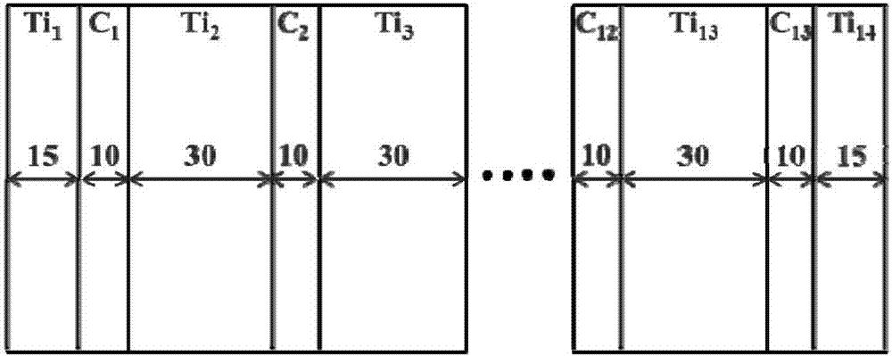
[0031] In this example, if figure 1 The silicon carbide ceramic materials to be joined are shown as being joined using the joining layer material. The material to be connected is exactly the same as that in Example 1. Connecting layer materials such as figure 2 As shown, it is a left and right stacked structure, including 14 layers of Ti films, and there is a carbon film between the adjacent titanium films. The thicknesses of the films are all 10nm, the total thickness of the intermediate connecting layer after lamination is 520nm, and TiC=1:0.6. The silicon carbide materials to be connected are connected together through the connection layer by using an external heat source to heat the connection. The method of heating connection with an external heat source is basically the same as that of Example 1, which is an electric field-assisted thermocompression connection, and the specific steps are as follows:

[0032] (1) Polish the silicon carbide surface to be connected wit...

Embodiment 3

[0036] In this example, if figure 1 The silicon carbide ceramic materials to be joined are shown as being joined using the joining layer material. The material to be connected is exactly the same as that in Example 1. The structure of the connection layer material is basically the same as that in Example 2, including 14 layers of Ti films, and a carbon film between adjacent titanium films. The only difference is that the thickness of the top and bottom titanium films is 2nm, the thickness of the rest of the titanium films is 4nm, the thickness of each carbon film is 2nm, and the total thickness of the intermediate connection layer after stacking is 78nm. The silicon carbide materials to be connected are connected together through the connection layer by using an external heat source to heat the connection. The method of heating connection with an external heat source is basically the same as that of Example 1, which is an electric field-assisted thermocompression connection,...


PUM

PropertyMeasurementUnit
thicknessaaaaaaaaaa
thicknessaaaaaaaaaa
thicknessaaaaaaaaaa

Abstract

The present invention provides a connection material for connecting silicon carbide ceramics. The connection material has a left-right stacked structure, and comprises at least two titanium layers, wherein a carbon layer is arranged between the adjacent titanium layers. According to the present invention, the connection material is sandwiched between silicon carbide ceramic materials to be connected, and the nanometer titanium layer and the nanometer carbon layer are subjected to an exothermic reaction when the SiC materials to be connected are integrally connected by heating the connection interface through an external heat source, such that the middle connection layer can release the partial heat so as to reduce the energy supply of the external heat source, easily save the cost, and reduce the industrial production difficulty.

Description

technical field [0001] The invention relates to the technical field of silicon carbide ceramic materials, in particular to a connection material for connecting silicon carbide ceramics, a preparation method thereof, and a method for connecting silicon carbide ceramics using the connection material Background technique [0002] Silicon carbide ceramics (SiC) have a series of advantages such as low neutron activity, strong resistance to neutron radiation, low density, high temperature resistance, oxidation resistance, and wear resistance, and are the first choice for a new generation of nuclear fuel cladding materials. However, the inherent defects of silicon carbide ceramics, the inherent brittleness and non-deformability of ceramic materials, and the processing and repair of parts make it very difficult to manufacture silicon carbide ceramics with complex shapes, so in actual manufacturing usually requires connection technology To realize the processing of complex ceramic pa...

Claims


Application Information

Patent Timeline
Patent Type & Authority Applications(China)
IPC IPC(8): C04B37/00C04B35/565
CPCC04B35/565C04B37/00
Inventor 黄庆杨辉周小兵黄峰都时禹
Owner NINGBO INST OF MATERIALS TECH & ENG CHINESE ACADEMY OF SCI
Learn More