Superconducting nanowire single photon detector
A single-photon detector and superconducting nanowire technology, applied in the field of light detection, can solve the problems of increasing dynamic inductance and decreasing device count rate, and achieve the effects of increasing current, reducing total inductance, and improving signal-to-noise ratio.
- Summary
- Abstract
- Description
- Claims
- Application Information
AI Technical Summary
Problems solved by technology
Method used
Image

Examples
Embodiment 1
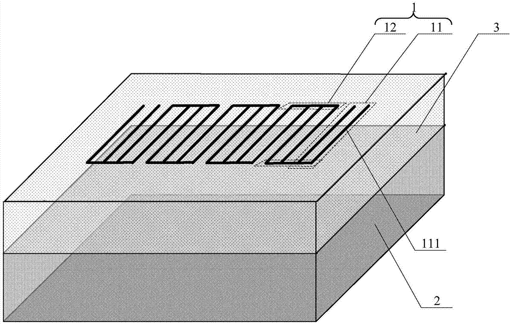
[0071] see Figure 1 to Figure 3 , the present embodiment provides a superconducting nanowire single photon detector, the superconducting nanowire single photon detector includes a layer of superconducting nanowire structure 1, and the superconducting nanowire structure 1 includes several parallel spaced rows The linear portion 11 of the cloth and the first connecting portion 12 connecting the linear portion 11 end to end in sequence; wherein, the linear portion 11 includes at least two superconducting nanowires 111 arranged in parallel at intervals, each of the linear portions 11 The superconducting nanowires 111 inside are connected via the first connecting portion 12 . In the present invention, the straight line portion 11 of the superconducting nanowire structure 1 is set as at least two superconducting nanowires 111 arranged in parallel at intervals, and the superconducting nanowires 111 in each straight line portion 11 pass through the When one of the superconducting na...
Embodiment 2
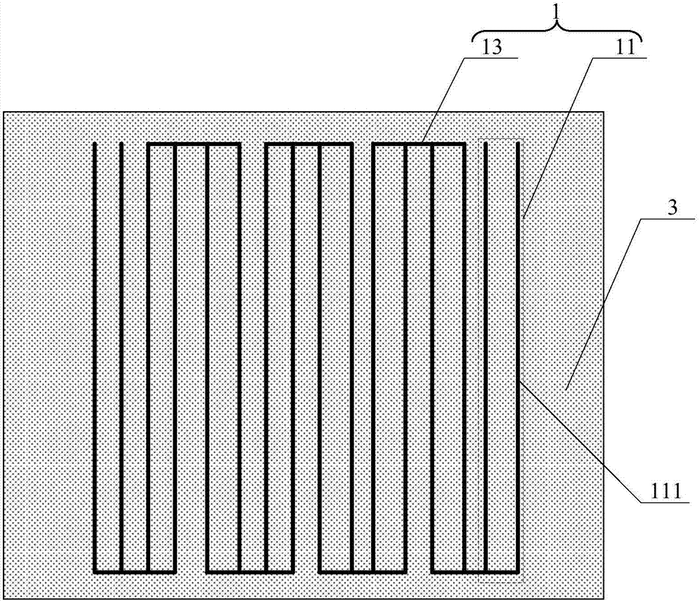
[0085] see Figure 4 to Figure 6 , this embodiment also provides a superconducting nanowire single photon detector, the specific structure of the superconducting nanowire single photon detector described in this embodiment is the same as that of the superconducting nanowire single photon detector described in Embodiment 1 The specific structures are roughly the same, and the difference between the two is that: compared with the superconducting nanowire structure 1 in the first embodiment, the superconducting nanowire structure 1 in this embodiment has a second connection part 13 added, and the The second connecting portion 13 is located in the straight line portion 11, and between the superconducting nanowires 111 arranged in parallel in the straight line portion 11, and connects the adjacent superconducting nanowires 111 in the straight line portion 11. The conductive nanowires 111 are connected. By adding the second connection part 13 in the superconducting nanowire structu...
Embodiment 3
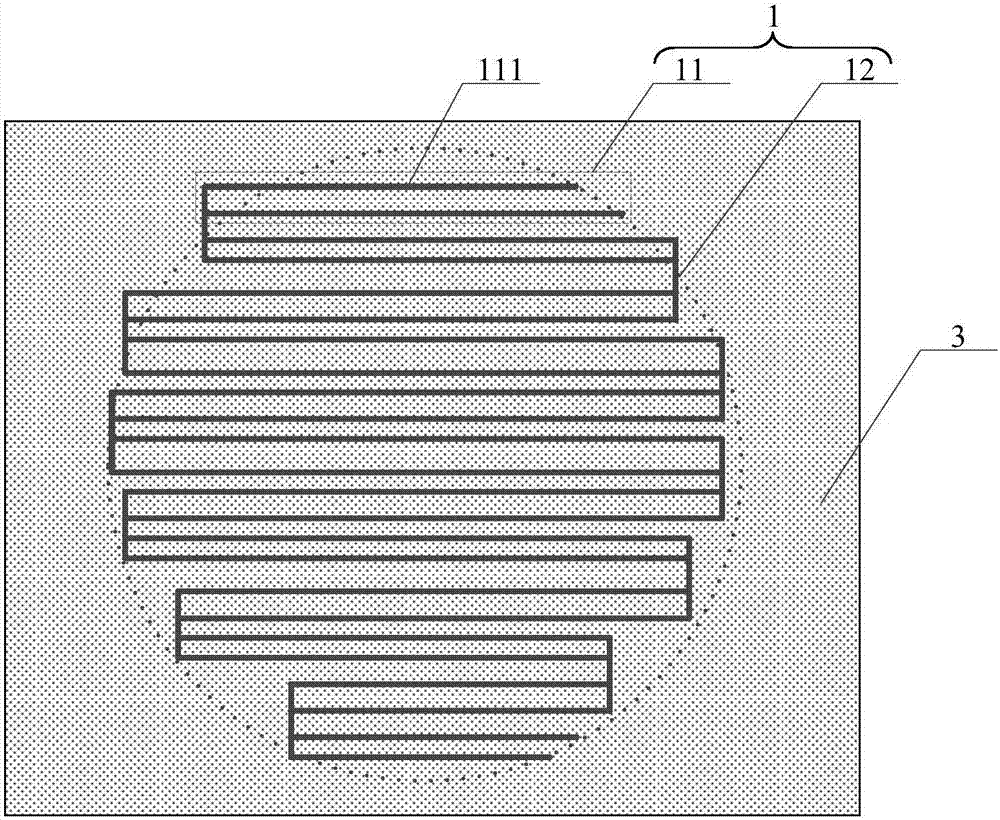
[0090] Please combine Figure 1 to Figure 3 refer to Figure 7 to Figure 9 , the present embodiment also provides a superconducting nanowire single photon detector, the superconducting nanowire single photon detector described in the present embodiment comprises: a substrate 2; an N-layer dielectric layer 4, the N-layer dielectric layer 4 are sequentially stacked on the upper surface of the substrate 2, wherein N is an integer ≥ 1; an N-layer superconducting nanowire structure 1, the superconducting nanowire structure 1 is located on the corresponding side of the dielectric layer 4 On the upper surface, and when N≥2, the superconducting nanowire structure 1 in the first N-1 layers is completely covered by the dielectric layer 4 on the upper layer.
[0091] As an example, the specific structure of the superconducting nanowire structure 1 is completely the same as that of the superconducting nanowire structure 1 described in the first embodiment, please refer to the first embod...
PUM
| Property | Measurement | Unit |
|---|---|---|
| Thickness | aaaaa | aaaaa |
| Thickness | aaaaa | aaaaa |
| Thickness | aaaaa | aaaaa |
Abstract
Description
Claims
Application Information
 - R&D
- Intellectual Property
- Life Sciences
- Materials
- Tech Scout
- Unparalleled Data Quality
- Higher Quality Content
- 60% Fewer Hallucinations
Browse by: Latest US Patents, China's latest patents, Technical Efficacy Thesaurus, Application Domain, Technology Topic, Popular Technical Reports.
© 2025 PatSnap. All rights reserved.Legal|Privacy policy|Modern Slavery Act Transparency Statement|Sitemap|About US| Contact US: help@patsnap.com