PI substrate, manufacturing method thereof and display device

A technology for display devices and substrates, applied in identification devices, semiconductor/solid-state device manufacturing, photovoltaic power generation, etc., can solve problems such as uneven edge thickness of PI films, achieve the effect of eliminating uneven edge thickness and improving yield

Active Publication Date: 2017-12-22
BOE TECH GRP CO LTD
View PDF10 Cites 0 Cited by
  • Summary
  • Abstract
  • Description
  • Claims
  • Application Information

AI Technical Summary

Problems solved by technology

[0004] The invention provides a PI substrate and its preparation method and display device to solve the problem of uneven edge thickness of the PI film existing when coating PI

Method used


Image

  • PI substrate, manufacturing method thereof and display device
  • PI substrate, manufacturing method thereof and display device
  • PI substrate, manufacturing method thereof and display device

Examples


Embodiment 1

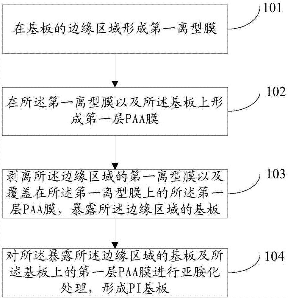
[0044] refer to figure 1 , which shows a flowchart of a method for preparing a PI substrate according to Embodiment 1 of the present invention.

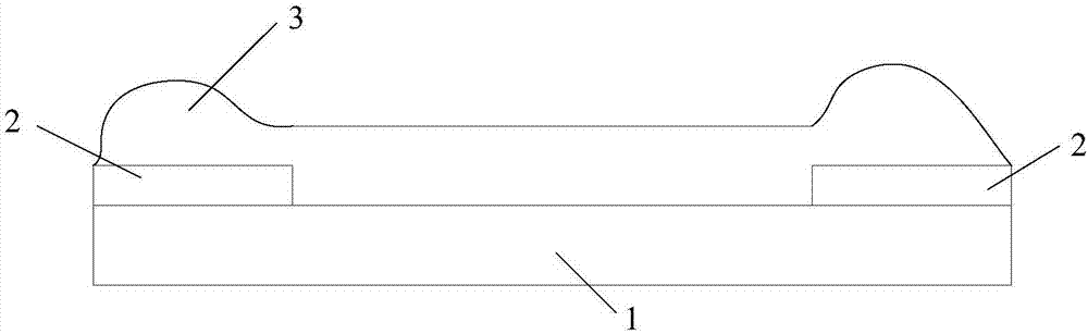
[0045] Step 101: forming a first release film on the edge region of the substrate, such as figure 2 shown.

[0046] A first release film 2 is formed on the edge region of the substrate 1, and the first release film 2 adopts a low-adhesion adhesive material, which is resistant to N-methyl-2-pyrrolidone (N-methyl-2-pyrrolidone, NMP) Solvent attack, and has heat resistance stability above 100°C.

[0047] The substrate can be formed of a transparent glass material whose main component is silicon dioxide. The material forming the substrate is not limited to the transparent glass material, and can also be a transparent plastic material. The substrate is preferably a glass substrate or a rigid substrate.

[0048] Step 102: Form a first layer of polyamic acid PAA film 3 on the first release film 2 and the substrate 1, such as image 3 s...

Embodiment 2

[0055] refer to Image 6 , which shows a flowchart of a method for preparing a PI substrate according to Embodiment 2 of the present invention.

[0056]Step 601: Form a first release film on the edge area of ​​the substrate.

[0057] The first release film adopts a low-adhesive adhesive material, which is resistant to erosion by N-methyl-2-pyrrolidone (NMP) solvents, and has a heat-resistant stability above 100°C. Since polyimide can be resistant to erosion and reaction, the first release film material includes at least one of polyimide and polypropylene.

[0058] The width of the first release film can be set according to actual needs, which is not specifically limited in the present invention, and the width of the first release film is preferably 10 mm.

[0059] Step 602: forming a first layer of PAA film on the first release film and the substrate.

[0060] Coating a PAA film on the first release film and the substrate; drying the PAA film at high temperature to form a h...

Embodiment 3

[0082] refer to figure 2 , which shows a structural block diagram of a PI substrate according to Embodiment 3 of the present invention.

[0083] a substrate comprising a central region and an edge region;

[0084] A first layer of PAA film, the first layer of PAA film is formed in the central area of ​​the substrate, wherein the flatness of the first layer of PAA film satisfies a preset condition.

[0085] The preset condition refers to that the flatness and thickness of the first PAA film are uniform.

[0086] Preferably, the PI substrate further includes: an inorganic layer covering the edge region of the substrate and the first layer of PAA film.

[0087] a second PAA film formed on the inorganic layer in the central region of the substrate.

[0088] In this embodiment, by forming a first release film in the edge area of ​​the substrate; forming a first layer of PAA film on the first release film and the substrate; peeling off the first release film in the edge area and...


PUM


Abstract

The invention provides a PI substrate, a manufacturing method thereof and a display device. The manufacturing method comprises the steps of: forming a first release film in an edge region of a substrate; forming a first layer of polyamic acid PAA film on the first release film and the substrate; stripping the first release film in the edge region and the first layer PAA film covering the first release film, and exposing the substrate in the edge region; and performing imidization processing on the exposed substrate in the edge region and the first layer PAA film on the substrate, so as to form a PI substrate. Therefore, the problem of uneven edge thickness of a PI film when coating the PI at present is solved.

Description

technical field [0001] The invention relates to the technical field of displays, in particular to a PI substrate, a preparation method thereof, and a display device. Background technique [0002] In recent years, with the rapid development of flexible display technology, various display panel manufacturers have exhibited their own prototypes, and are also actively planning their own flexible display production lines and mass production lines. Flexible display technology has gradually moved from research and development to mass production, making flexible display technology developed rapidly. [0003] At present, flexible substrates are divided into two types, one is a sandwich structure polyimide (Polyimide, PI) substrate, and the other is a single-layer PI substrate. When the above two PI substrates are coated with polyimide PI, due to The PI diffusion is not uniform, resulting in regions of non-uniform film thickness at the edge of the PI substrate. Due to the uneven thi...

Claims


Application Information

Patent Timeline
Patent Type & Authority Applications(China)
IPC IPC(8): H01L51/00G09F9/30
CPCG09F9/301H10K77/111H01L27/1218H01L27/1266Y02E10/549G06F1/1652H01L27/124H10K59/00
Inventor 郭远征谢明哲宋平王有为代伟男汪明文
Owner BOE TECH GRP CO LTD
Why Eureka
Try Eureka