

A thin film patterning method on a flexible substrate
A technology for flexible substrates and thin-film graphics, which is applied in the direction of gaseous chemical plating, photolithography on patterned surfaces, and techniques for producing decorative surface effects. Problems such as the difficulty of thin film material layers, to achieve the effect of expanding the range of thin film materials, avoiding process steps, and eliminating side etching
Active Publication Date: 2012-07-18
NORTHWESTERN POLYTECHNICAL UNIV
View PDF0 Cites 4 Cited by
- Summary
- Abstract
- Description
- Claims
- Application Information
AI Technical Summary
Problems solved by technology
The above method has the following disadvantages: 1) Unlike the hard and smooth rigid substrate, it is not easy to spin-coat liquid photoresist evenly and smoothly on the flexible substrate, thereby affecting the exposure accuracy and the patterning effect of the film; 2) on the flexible substrate The excess film material layer is not easy to be removed by etching, because during the film material deposition process, the energetic film material particles are easily injected under the surface layer of the flexible substrate with low hardness, so that the gap between the flexible substrate and the film material layer The blurring of the interface increases the difficulty of etching and removing the excess thin film material layer; 3) thin film etching is only suitable for some materials, and some materials such as those that are difficult to etch by chemical etching or other means are not suitable for this method; 4) When the same film layer involves different material regions, the etching medium and etching protection will affect each other; 5) If the patterned line feature size is required to be very fine, the side etching phenomenon caused by the etching process cannot be ignored
Method used
View moreImage
Smart ImageViewing Examples

Examples
Embodiment 1
Embodiment 2
Login to View More PUM
 Abstract
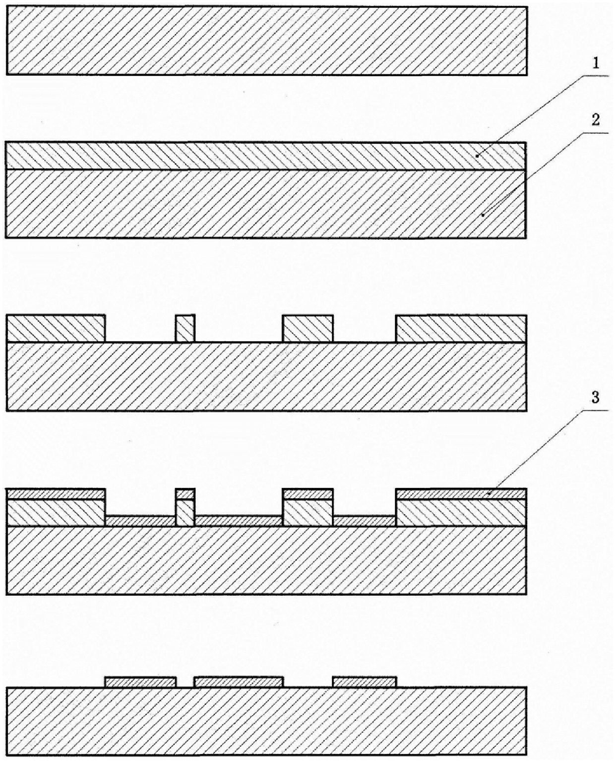
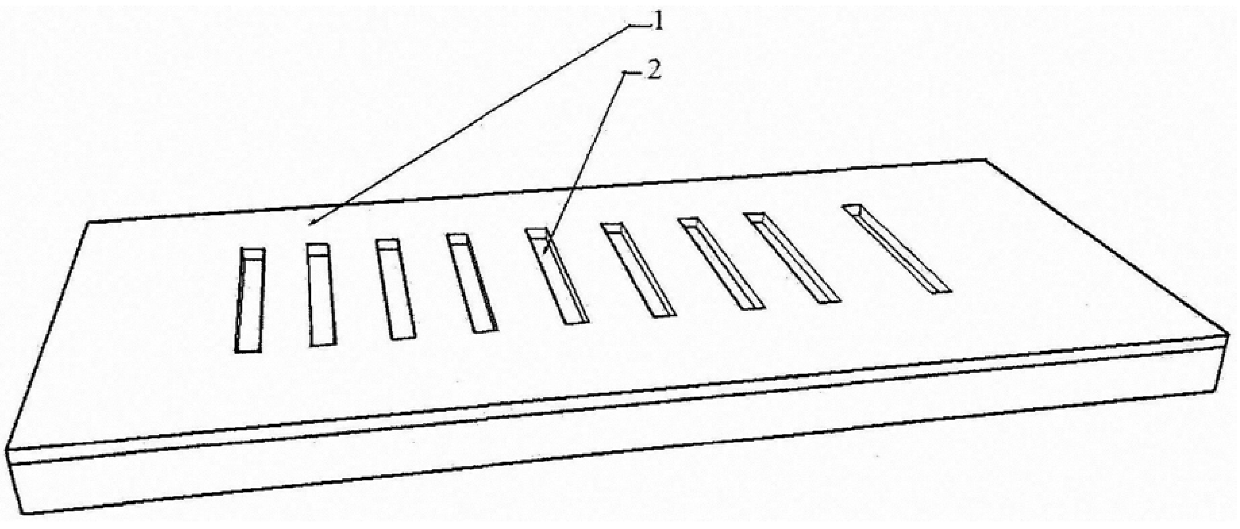
The invention discloses a film patterning method on a flexible substrate, which belongs to the field of microprocessing. This method directly attaches the entire dry film for photolithographic exposure, avoiding the problem of poor flatness and uniformity caused by spin-coating liquid photoresist on the flexible substrate that affects the exposure accuracy, and also avoids the curing of liquid photoresist, etc. Complicated process steps; using the lift-off method instead of the etching process, the film to be removed is not directly deposited on the flexible substrate but separated by a dry film layer, which avoids the injection of the film material into the softer flexible substrate layer, so the final removal This part of the film is easier and more thorough, and at the same time it is suitable for forming films of difficult-to-etch materials, expanding the range of film materials and eliminating problems such as side etching.
Description
Technical field: The invention belongs to the field of microfabrication, in particular to a film patterning method on a flexible substrate. Background technique: Microfabrication on flexible substrates can obtain functional thin film patterns, which can be used as functional structures or devices such as thin film sensor probes, resistors, electrodes, heaters, wires, etc., and have overall flexibility and bendability, thin thickness, and feature size Small, easy to array and so on. Especially when it is used as a miniature sensor probe, it can realize precise, fast and distributed measurement tasks, and can fully adapt to the measurement tasks on the surface of non-planar objects with high curvature. The patterning of thin films on flexible substrates generally follows the thin film patterning method on hard substrates, that is, etching or etching process-a method of obtaining patterned thin films by etching and removing unmasked and protected exposed thin film materials. ...
Claims
Login to View More Application Information
Patent Timeline
 IPC IPC(8): G03F7/00B81C1/00H05K3/18
Inventor马炳和傅博任进忠邓进军姜澄宇马志波叶芳
OwnerNORTHWESTERN POLYTECHNICAL UNIV